 | –≠–ª–µ–∫—Ç—Ä–æ–Ω–Ω—ã–π –∫–æ–º–ø–æ–Ω–µ–Ω—Ç: LM34910SD | –°–∫–∞—á–∞—Ç—å:  PDF PDF  ZIP ZIP |
LM34910
High Voltage (40V, 1.25A) Step Down Switching
Regulator
General Description
The LM34910 Step Down Switching Regulator features all of
the functions needed to implement a low cost, efficient, buck
bias regulator capable of supplying 1.25A to the load. This
buck regulator contains a 40V N-Channel Buck Switch, and
is available in the thermally enhanced LLP-10 package. The
hysteretic regulation scheme requires no loop compensa-
tion, results in fast load transient response, and simplifies
circuit implementation. The operating frequency remains
constant with line and load variations due to the inverse
relationship between the input voltage and the on-time. The
current limit detection is set at 1.25A. Additional features
include: VCC under-voltage lockout, thermal shutdown, gate
drive under-voltage lockout, and maximum duty cycle limiter.
Features
n
Integrated 40V, N-Channel buck switch
n
Integrated start-up regulator
n
Input Voltage Range: 8V to 36V
n
No loop compensation required
n
Ultra-Fast transient response
n
Operating frequency remains constant with load current
and input voltage
n
Maximum Duty Cycle Limited During Start-Up
n
Adjustable output voltage
n
Valley Current Limit At 1.25A
n
Precision internal reference
n
Low bias current
n
Highly efficient operation
n
Thermal shutdown
Typical Applications
n
High Efficiency Point-Of-Load (POL) Regulator
n
Non-Isolated Telecommunication Buck Regulator
n
Secondary High Voltage Post Regulator
Package
n
LLP-10 (4 mm x 4 mm)
n
Exposed Thermal Pad For Improved Heat Dissipation
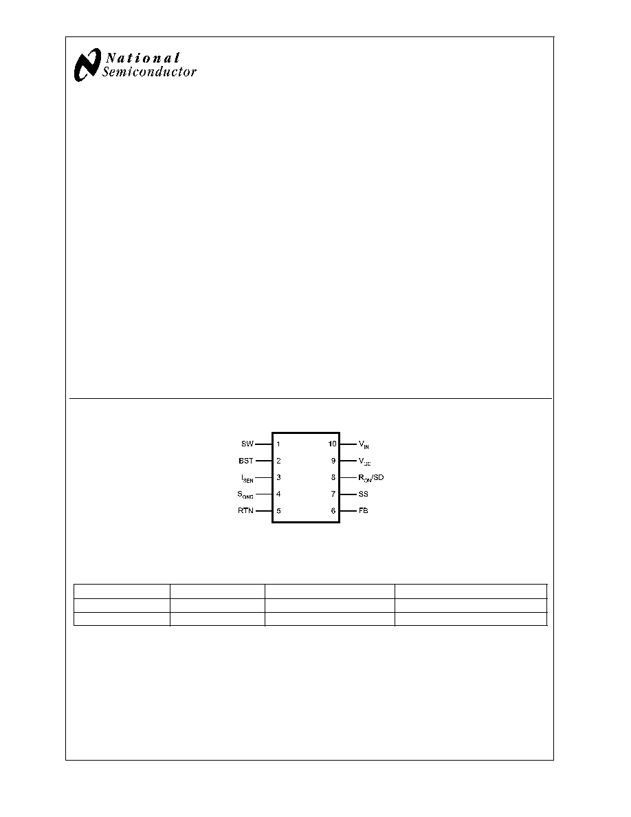
Connection Diagram
20110902
10-Lead LLP
Ordering Information
Order Number
Package Type
NSC Package Drawing
Supplied As
LM34910SD
LLP-10 (4x4)
SDC10A
1000 Units on Tape and Reel
LM34910SDX
LLP-10 (4x4)
SDC10A
4500 Units on Tape and Reel
February 2005
LM34910
High
V
oltage
(40V
,
1.25A)
Step
Down
Switching
Regulator
© 2005 National Semiconductor Corporation
DS201109
www.national.com
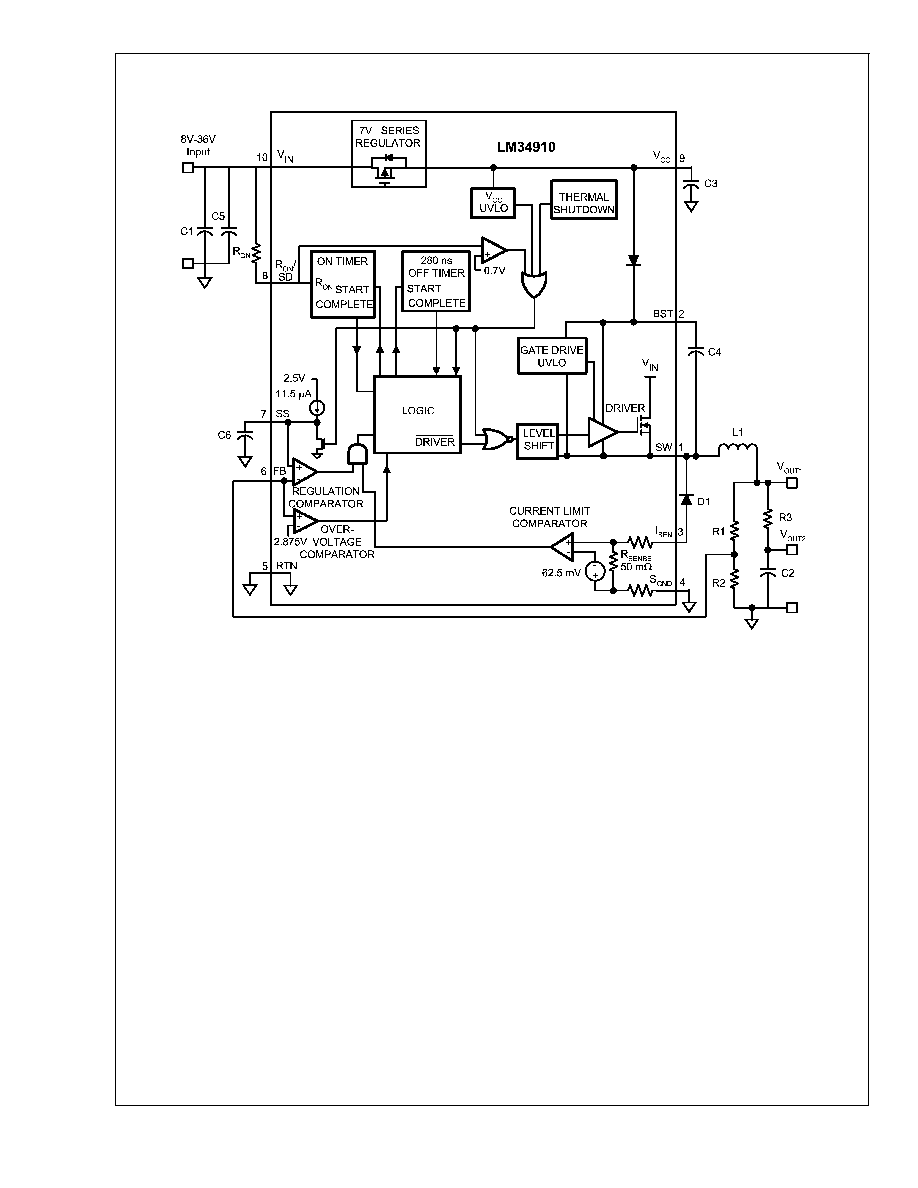
Typical Application Circuit and Block Diagram
20110901
FIGURE 1.
LM34910
www.national.com
2
Pin Description
PIN
NAME
DESCRIPTION
APPLICATION INFORMATION
1
SW
Switching Node
Internally connected to the buck switch source.
Connect to the external inductor, diode, and boost
capacitor.
2
BST
Boost pin for boot-strap capacitor
Connect a 0.022 µF capacitor from SW to this pin. An
internal diode charges the capacitor during the
off-time.
3
I
SEN
Current sense input
Internally the current sense resistor connects from this
pin to S
GND
. Re-circulating current flows out of this pin
to the free-wheeling diode. Current limit is set at
1.25A.
4
S
GND
Sense Ground
Re-circulating current flows into this pin to the current
sense resistor.
5
RTN
Circuit Ground
Ground for all internal circuitry other than the current
limit detection.
6
FB
Feedback
Internally connected to the regulation and over-voltage
comparators. The regulation level is 2.5V.
7
SS
Softstart
An internal 11.5 µA current source charges an external
capacitor to 2.5V to provide the softstart function.
8
R
ON
/SD
On-time Control and Shutdown
An external resistor from V
IN
to this pin sets the buck
switch on-time. Grounding this pin shuts down the
regulator.
9
V
CC
Output from the start-up regulator
Nominally regulated to 7.0V. An external voltage
(8V-14V) can be connected to this pin to reduce
internal dissipation. An internal diode connects V
CC
to
V
IN
.
10
V
IN
Input supply voltage
Nominal input range is 8.0V to 36V.
LM34910
www.national.com
3
Absolute Maximum Ratings
(Note 1)
If Military/Aerospace specified devices are required,
please contact the National Semiconductor Sales Office/
Distributors for availability and specifications.
V
IN
to GND
40V
BST to GND
50V
SW to GND (Steady State)
-1.5V
ESD Rating (Note 2)
Human Body Model
2kV
BST to V
CC
40V
V
IN
to SW
40V
BST to SW
14V
V
CC
to GND
14V
S
GND
to RTN
-0.3V to +0.3V
Current out of I
SEN
See Text
SS to RTN
-0.3V to 4V
All Other Inputs to GND
-0.3 to 7V
Storage Temperature Range
-55∞C to +150∞C
JunctionTemperature
150∞C
Operating Ratings
(Note 1)
V
IN
8.0V to 36V
Junction Temperature
-40∞C to + 125∞C
Electrical Characteristics
Specifications with standard typeface are for T
J
= 25∞C, and those with boldface
type apply over full Operating Junction Temperature range. V
IN
= 24V, R
ON
= 200k unless otherwise stated (Note 5).
Symbol
Parameter
Conditions
Min
Typ
Max
Units
Start-Up Regulator, V
CC
V
CC
Reg
V
CC
regulated output
6.6
7
7.4
V
V
IN
-V
CC
dropout voltage
I
CC
= 0 mA,
V
CC
= V
CC
Reg - 100 mV
1.4
V
V
CC
output impedance
0 mA
I
CC
5 mA
140
V
CC
current limit (Note 3)
V
CC
= 0V
9
mA
UVLO
VCC
V
CC
under-voltage lockout
threshold
V
CC
increasing
5.8
V
UVLO
VCC
hysteresis
V
CC
decreasing
150
mV
UVLO
VCC
filter delay
100 mV overdrive
3
µs
I
IN
operating current
Non-switching, FB = 3V
0.63
1
mA
I
IN
shutdown current
R
ON
/SD = 0V
80
250
µA
Switch Characteristics
Rds(on)
Buck Switch Rds(on)
I
TEST
= 200 mA
0.45
0.95
UVLO
GD
Gate Drive UVLO
V
BST
- V
SW
Increasing
3.0
4.3
5.5
V
UVLO
GD
hysteresis
440
mV
Softstart Pin
Pull-up voltage
2.5
V
Internal current source
11.5
µA
Current Limit
I
LIM
Threshold
Current out of I
SEN
1
1.25
1.5
A
Resistance from I
SEN
to S
GND
130
m
Response time
150
ns
On Timer
t
ON
- 1
On-time
V
IN
= 10V, R
ON
= 200 k
2.1
2.75
3.6
µs
t
ON
- 2
On-time
V
IN
= 36V, R
ON
= 200 k
740
ns
Shutdown threshold
Voltage at R
ON
/SD rising
0.35
0.65
1.1
V
Threshold hysteresis
Voltage at R
ON
/SD falling
40
mV
Off Timer
t
OFF
Minimum Off-time
280
ns
Regulation and Over-Voltage Comparators (FB Pin)
V
REF
FB regulation threshold
SS pin = steady state
2.440
2.5
2.550
V
FB over-voltage threshold
2.875
V
FB bias current
100
nA
LM34910
www.national.com
4
Electrical Characteristics
Specifications with standard typeface are for T
J
= 25∞C, and those with boldface
type apply over full Operating Junction Temperature range. V
IN
= 24V, R
ON
= 200k unless otherwise stated (Note
5). (Continued)
Symbol
Parameter
Conditions
Min
Typ
Max
Units
Thermal Shutdown
T
SD
Thermal shutdown
temperature
175
∞C
Thermal shutdown hysteresis
20
∞C
Note 1: Absolute Maximum Ratings are limits beyond which damage to the device may occur. Operating Ratings are conditions under which operation of the device
is intended to be functional. For guaranteed specifications and test conditions, see the Electrical Characteristics.
Note 2: The human body model is a 100pF capacitor discharged through a 1.5k
resistor into each pin.
Note 3: V
CC
provides self bias for the internal gate drive and control circuits. Device thermal limitations limit external loading
Note 4: For detailed information on soldering plastic LLP packages, refer to the Packaging Data Book available from National Semiconductor Corporation.
Note 5: Typical specifications represent the most likely parametric norm at 25∞C operation.
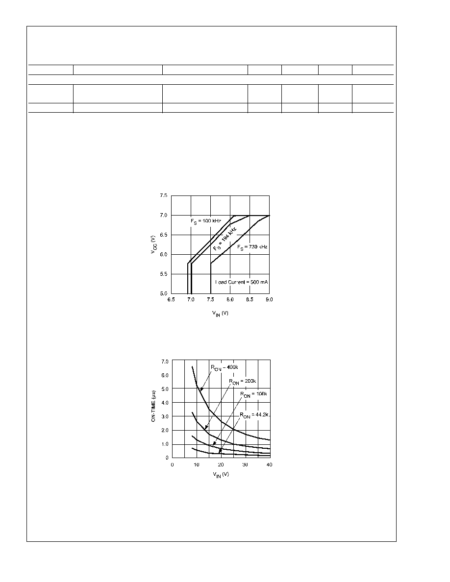
Typical Performance Characteristics
20110904
FIGURE 2. V
CC
vs V
IN
20110905
FIGURE 3. ON-Time vs V
IN
and R
ON
LM34910
www.national.com
5