 | –≠–ª–µ–∫—Ç—Ä–æ–Ω–Ω—ã–π –∫–æ–º–ø–æ–Ω–µ–Ω—Ç: LM3495 | –°–∫–∞—á–∞—Ç—å:  PDF PDF  ZIP ZIP |
LM3495
Emulated Peak Current Mode Buck Controller for Low
Output Voltage
General Description
The LM3495 is a PWM buck regulator which implements a
unique emulated peak current mode control. This control
method eliminates the switching noise which typically limits
current mode operation at extremely short duty cycles and
high operating frequency. The switching frequency is pro-
grammable between 200 kHz and 1.5 MHz, and can also be
synchronized to an external clock. The LM3495 is also very
fault tolerant with both switch node short, hiccup mode, and
adaptive duty cycle limit protection. A 0.6V 1% reference and
glitch free pre-biased start-up ensure the most demanding
digital loads operate reliably. Internal soft start and the ability
to track the output of another supply make the LM3495
versatile and efficient.
Features
n
Input voltage from 2.9V to 18V
n
Output voltage adjustable from 0.6V to 5.5V
n
Feedback Accuracy:
±
1%
n
Low-side Sensing, Programmable Current Limit without
sense resistor
n
Input Under Voltage Lockout
n
Hiccup mode current limit protection eliminates thermal
runaway during fault conditions
n
Internal soft start with tracking capability
n
200 kHz to 1.5 MHz Switching frequency,
Synchronizable
n
On-chip gate drivers
n
Soft output discharge during shutdown
n
Startup into output pre-bias
n
Operation from a single input rail
n
Adaptive Duty Cycle Limit
n
TSSOP-16 package
Applications
n
Wide input voltage buck converters with low voltage,
high accuracy outputs
n
Core logic regulators
n
High-efficiency buck regulation
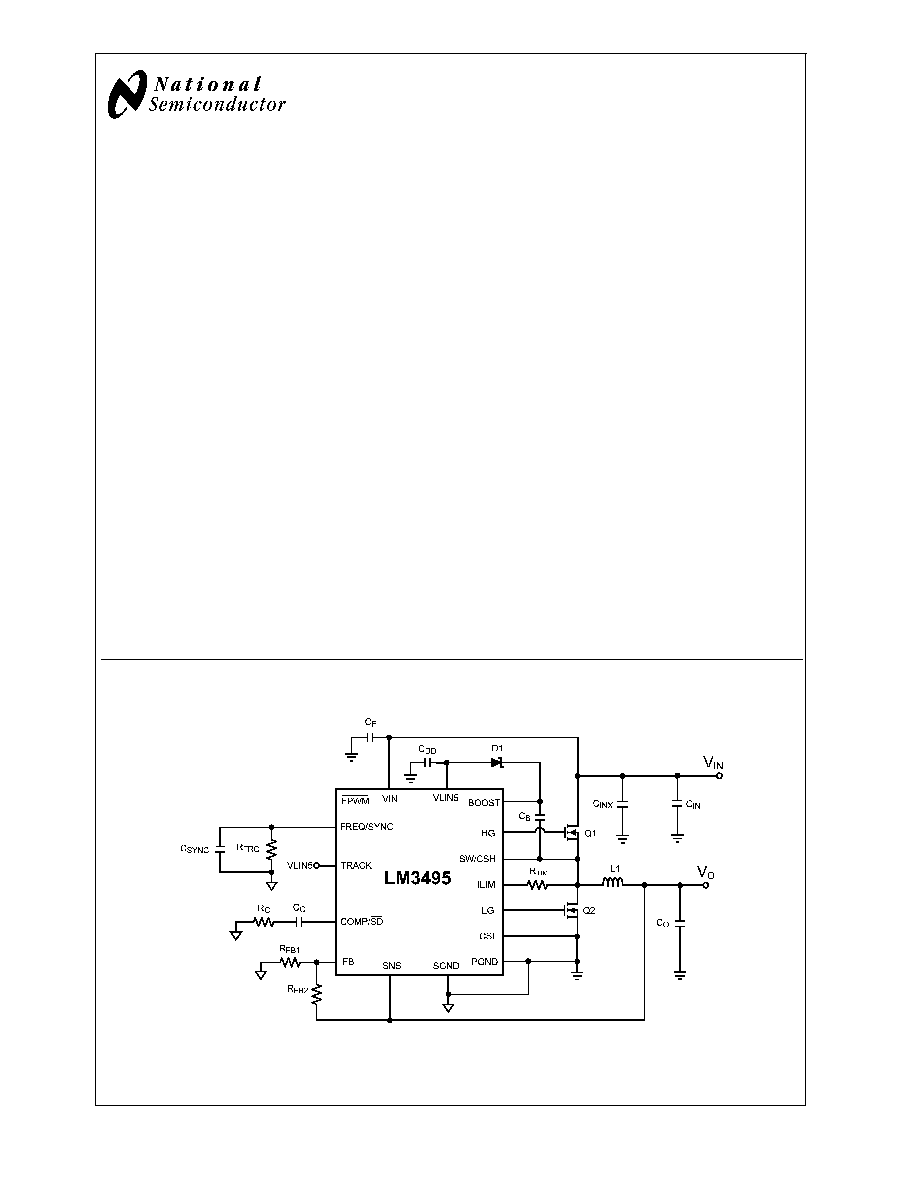
Typical Application
20169901
April 2006
LM3495
Emulated
Peak
Current
Mode
Buck
Controller
for
Low
Output
V
oltage
© 2006 National Semiconductor Corporation
DS201699
www.national.com
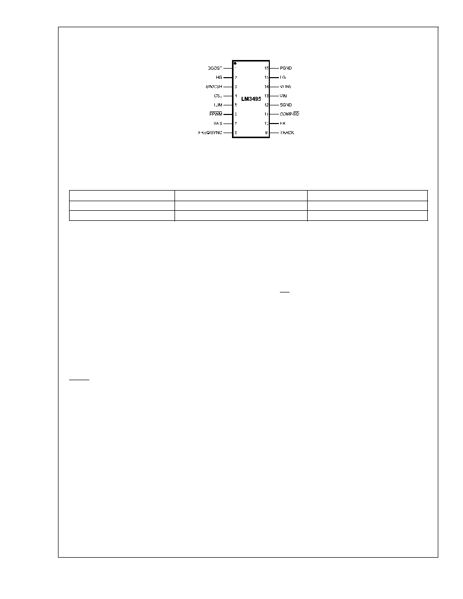
Connection Diagram
TOP VIEW
20169902
16-Lead Plastic TSSOP
JA
= 155∞C/W
Ordering Information
Part Number
NSC Package Drawing
Supplied As
LM3495MTC
MTC16
92 Units Per Rail
LM3495MTCX
MTC16
2.5k Units Per Reel
Pin Descriptions
BOOST (Pin 1): Supply rail for the high-side FET gate drive.
The voltage should be at least one gate threshold above the
regulator input voltage to properly turn on the high-side FET.
HG (Pin 2): Gate drive for the high-side N-channel FET. This
signal is interlocked with LG to avoid shoot-through.
SW/CSH (Pin 3): Return path for the high-side FET driver
and top Kelvin sense point for the load current. Connect this
pin as close as possible to the drain of the low-side FET with
a separate trace. Also used along with CSL for zero crossing
detection.
CSL (Pin 4): Bottom sense point for the load current. Con-
nect this as close as possible to the source of the low-side
FET with a separate trace.
ILIM (Pin 5): Current limit threshold setting. This pin sources
a fixed 20 µA current. A resistor of appropriate value should
be connected between this pin and the drain of the low-side
FET.
FPWM (Pin 6): Control mode select. An open circuit at this
pin allows the IC to operate in skip mode at light loads. A
logic low or connection to ground forces PWM operation at
all times. This pin should not be pulled up to any voltage
above 3.0V.
SNS (Pin 7): Output voltage sense pin. Connect this pin as
close as possible to the positive terminal of the output ca-
pacitor with a separate trace. This pin connects to an internal
FET that discharges the output capacitor during shutdown.
FREQ/SYNC (Pin 8): Switching frequency select pin and
input for external clock. Connect a resistor from this pin to
ground to determine switching frequency. Alternatively, a
logic level clock signal between 200 kHz and 1.5 MHz can be
applied to this pin through a 100 pF DC blocking capacitor to
set the switching frequency.
TRACK (Pin 9): Tracking pin. To force the output of the
LM3495 to track another power supply, connect a resistor
divider (smaller than 10 k
for better precision) from the
output of the other supply directly to this pin. When not used,
this pin should be connected directly to the VLIN5 pin.
FB (Pin 10): Feedback pin. Connecting a resistor divider
from the output voltage to this pin sets the DC level of the
output voltage.
COMP/SD (Pin 11): Output of the error amplifier. The volt-
age level on this pin is compared with an internally gener-
ated ramp signal to determine the duty cycle. This pin is
necessary for compensating the control loop. This pin must
be left floating for the converter to regulate the output voltage
in steady state. Forcing this pin below 0.3V shuts down the
regulator.
SGND (Pin 12): Signal ground. Ground connection for the
low power analog circuitry. Connect this pin to the PGND pin
with a separate trace.
VIN (Pin 13): Input voltage. Input to an internal 4.7V linear
regulator. Bypass this pin with a minimum 1 µF ceramic
capacitor.
VLIN5 (Pin 14): Output of the internal 4.7V linear regulator.
Provides power to the high-side bootstrap and low-side
driver. Bypass this pin with a 2.2 µF ceramic capacitor to
PGND.
LG (Pin 15): Gate drive for the low-side N-channel FET. This
signal is interlocked with HG to avoid shoot-through.
PGND (Pin 16): Ground connection for the power circuitry.
Connect to the source of the low-side FET and the output
capacitor with heavy traces or a copper plane.
LM3495
www.national.com
2
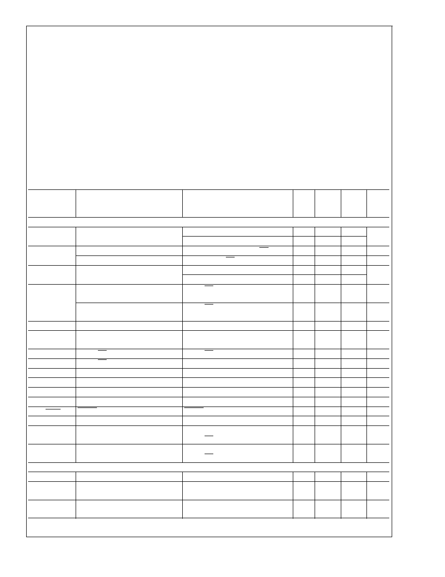
Absolute Maximum Ratings
(Note 1)
If Military/Aerospace specified devices are required,
please contact the National Semiconductor Sales Office/
Distributors for availability and specifications.
VIN, ILIM
-0.3V to 20V
SW/CSH (Note 5)
-0.5V to 20V
BOOST, HG
-0.3V to 25V
BOOST to SW
-0.3V to 6V
FB
-0.3V to 2V
TRACK, FREQ, FPWM, VLIN5,
SNS, LG, CSL
-0.3V to 6V
Storage Temperature
-65∞C to +150∞C
Soldering Information
Lead Temperature (soldering, 10
sec)
260∞C
Infrared or Convection (15 sec)
235∞C
ESD Rating (Note 2)
2kV
Operating Ratings
(Note 1)
Supply Voltage Range (V
IN
)
2.9V to 18V
BOOST to SW
2.5V to 5.5V
Junction Temperature
-40∞C to +125∞C
Electrical Characteristics
Specifications with standard type are for T
J
= 25∞C only; limits in boldface type
apply over the full Operating Junction Temperature (T
J
) range. Minimum and Maximum limits are guaranteed through test,
design, or statistical correlation. Typical values represent the most likely parametric norm at T
J
= 25∞C, and are provided for
reference purposes only. Unless otherwise indicated, V
IN
= 12V.
Symbol
Parameter
Conditions
Min
Typ
(Note
4)
Max
Units
SYSTEM PARAMETERS
V
FB
FB Pin Voltage
-20∞C to 85∞C
0.594
0.6
0.606
V
-40∞C to 125∞C
0.591
0.6
0.609
V
FB
/V
FB
Line Regulation
2.9V
<
VIN
<
18V, COMP/SD = 1.5V
0.1
%
Load Regulation
1.1V
<
COMP/SD
<
1.8V
0.1
%
V
ON
UVLO Thresholds
VIN Rising
2.55
2.6
2.7
V
VIN Falling
2.26
2.3
2.45
I
Q
Operating VIN Current
COMP/SD
>
0.3V
Not switching
1.8
mA
Quiescent Current
COMP/SD
<
0.3V
Shutdown, VIN = 18V
33
µA
I
ILIM
ILIM Pin Source Current
18
20
22
µA
V
ILIM-MAX
Maximum Current Limit Sense
Voltage
200
mV
I
SD
COMP/SD Pin Pull-up current
COMP/SD = 0V
2
2.6
µA
V
HICCUP
COMP/SD Pin Hiccup Threshold
2
V
t
DELAY
Hiccup Delay
16
Cycles
t
COOL
Cool Down Time Until Restart
4096
Cycles
t
SS
Internal Soft start Time
400
Cycles
V
OVP
Over Voltage Protection Threshold
As a % of nominal output voltage
116
125
132
%
I
FPWM
FPWM Pin Pull-up Current
FPWM = 0V
4.5
µA
V
FPWM-LO
FPWM Operation Threshold
FPWM Voltage Falling
0.9
V
R
SNS
SNS Pin Input Resistance
SNS = 1.5V
COMP/SD
>
0.3V
30
k
R
DIS
SNS Pin Discharge FET R
DSON
SNS = 1.5V
COMP/SD = 0V
350
440
530
GATE DRIVE
I
BOOST
BOOST Pin Leakage Current
BOOST - SW = 5.5V
25
nA
R
DS1
High-Side FET Driver Pull-up ON
resistance
BOOST - SW = 4.5V
4.5
R
DS2
High-Side FET Driver Pull-down ON
resistance
BOOST - SW = 4.5V
0.9
LM3495
www.national.com
3
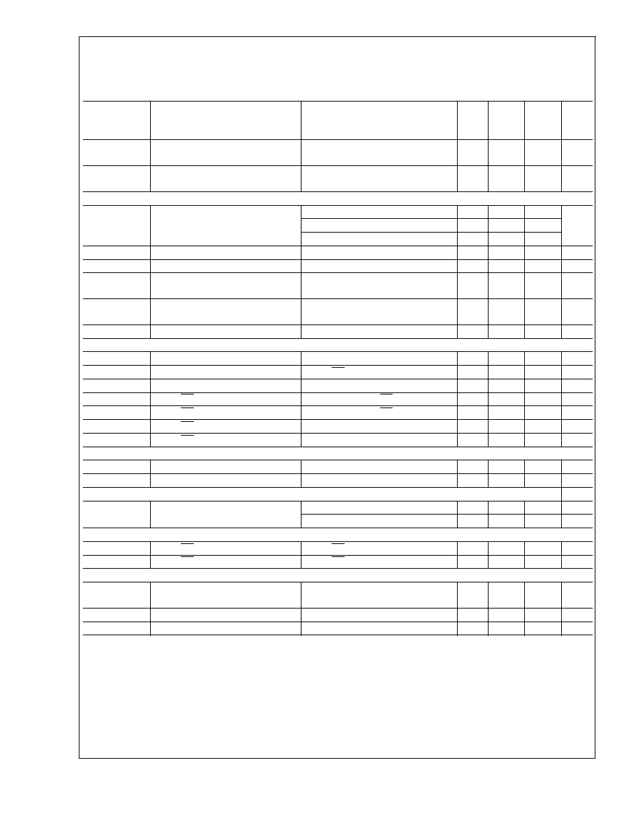
Electrical Characteristics
Specifications with standard type are for T
J
= 25∞C only; limits in boldface type
apply over the full Operating Junction Temperature (T
J
) range. Minimum and Maximum limits are guaranteed through test,
design, or statistical correlation. Typical values represent the most likely parametric norm at T
J
= 25∞C, and are provided for
reference purposes only. Unless otherwise indicated, V
IN
= 12V. (Continued)
Symbol
Parameter
Conditions
Min
Typ
(Note
4)
Max
Units
R
DS3
Low-Side FET Driver Pull-up ON
resistance
VLIN5 = 5.5V
1.4
R
DS4
Low-Side FET Driver Pull-down ON
resistance
VLIN5 = 5.5V
0.7
OSCILLATOR
f
SW
PWM Frequency
R
ADJ
= 150 k
200
kHz
R
ADJ
= 54.9 k
450
500
550
R
ADJ
= 17.8 k
1500
V
SYNC-HI
Threshold for SYNC on FREQ Pin
SYNC Voltage Rising
1.2
V
V
SYNC-LO
Threshold for SYNC on FREQ Pin
SYNC Voltage Falling
0.3
V
t
ON-SKIP
On Time During Skip Mode
V
O
= 1.5V
f
SW
= 500 kHz
125
ns
t
ON-MAX
Adaptive Maximum On-time Limit
V
O
= 1.5V
f
SW
= 500 kHz
750
ns
t
OFF-MIN
Minimum Off-time
300
ns
ERROR AMP
g
M
Transconductance
750
µmho
BW
-3dB
Open Loop Bandwidth
COMP/SD Floating
5
MHz
I
FB
FB Pin Bias Current
V
FB
= 0.6V
1
nA
I
SOURCE
COMP/SD Pin Source Current
V
FB
= 0.5V, COMP/SD = 1.5V
40
µA
I
SINK
COMP/SD Pin Sink Current
V
FB
= 0.7V, COMP/SD = 1.5V
40
µA
V
COMP-HI
COMP/SD Pin Voltage High Clamp
V
FB
= 0.5V
2
V
V
COMP-LO
COMP/SD Pin Voltage Low Clamp
V
FB
= 0.7V
0.9
V
TRACKING
V
TEND
Track End Threshold
0.6
V
V
TRACK-OS
Track to FB Offset
TRACK = 0.55V
15
mV
INTERNAL VOLTAGE REGULATOR
V
VLIN5
Voltage at VLIN5 Pin (Note 3)
V
IN
= 12V, VLIN5 Current = 25 mA
4.72
V
V
IN
= 3.3V, VLIN5 Current = 25 mA
3.0
V
LOGIC INPUTS AND OUTPUTS
V
SD-HI
COMP/SD Pin Logic High Trip Point
COMP/SD Pin Voltage Rising
0.3
0.4
V
V
SD-LO
COMP/SD Pin Logic Low Trip Point
COMP/SD Pin Voltage Falling
0.2
0.26
V
THERMAL CHARACTERISTICS
JA
Junction-to-Ambient Thermal
Resistance
155
∞C/W
T
SD
Thermal Shutdown Threshold
150
∞C
T
SD-HYS
Thermal Shutdown Hysteresis
15
∞C
Note 1: Absolute Maximum Ratings are limits beyond which damage to the device may occur. Operating Ratings are conditions under which operation of the device
is intended to be functional. For guaranteed specifications and test conditions, see the Electrical Characteristics.
Note 2: The human body model is a 100 pF capacitor discharged through a 1.5 k
resistor into each pin.
Note 3: VLIN5 provides self bias for the internal gate drive and control circuits. Device thermal limitations limit external loading.
Note 4: Typical specifications represent the most likely parametric norm at 25∞C operation.
Note 5: An extended negative voltage limit of ≠2V applies for a duration of 20 ns per switching cycle
LM3495
www.national.com
4
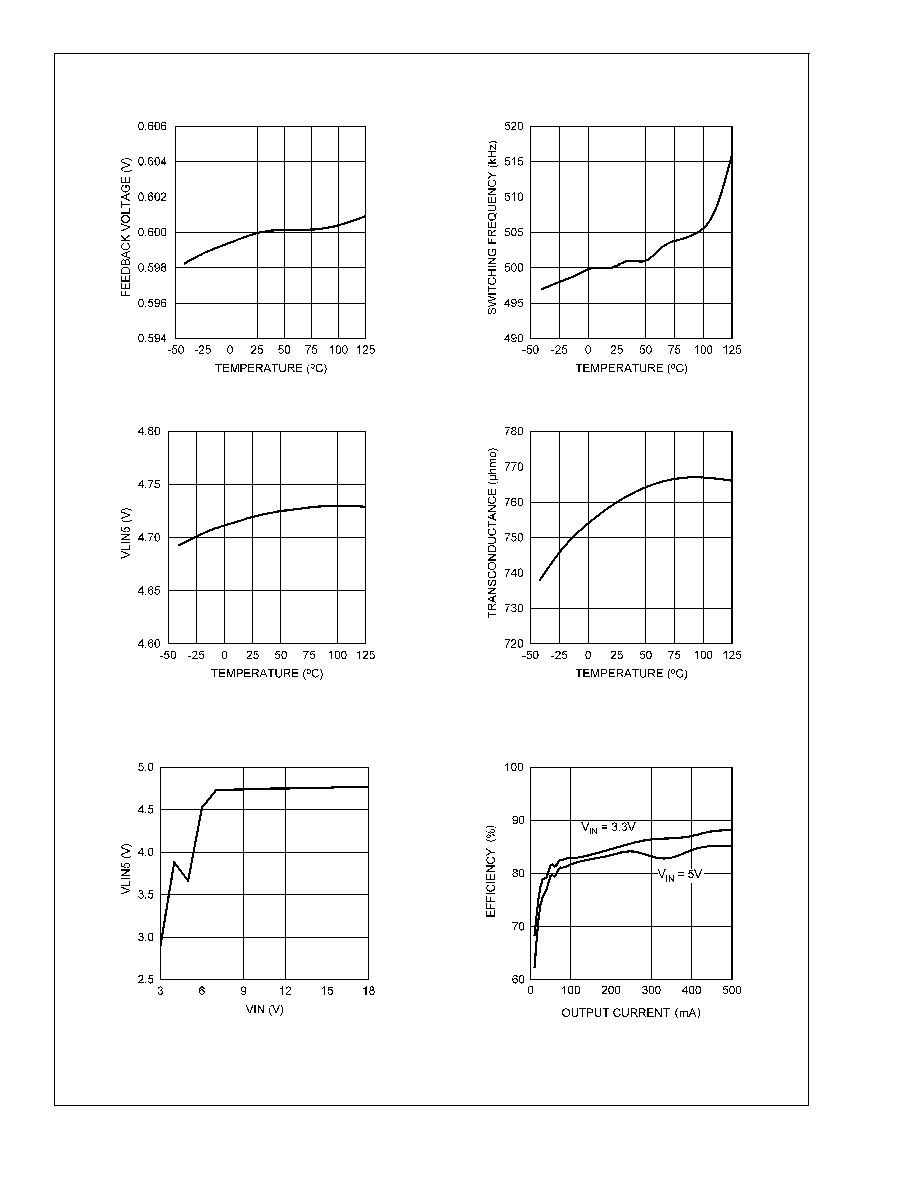
Typical Performance Characteristics
V
IN
= 12V unless specified, T
A
= 25∞C unless specified.
FB Reference Voltage vs Temperature
Switching Frequency vs Temperature
20169903
20169904
VLIN5 Voltage vs Temperature
Error Amplifier Transconductance vs Temperature
20169905
20169906
VLIN5 Voltage vs VIN
Efficiency in SKIP Mode
V
O
= 2.2V, I
O
= 10 mA to 500 mA
BOM in Table 2
20169908
20169912
LM3495
www.national.com
5