LM3500
Synchronous Step-up DC/DC Converter for White LED
Applications
General Description
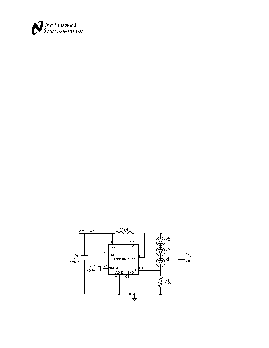
The LM3500 is a fixed-frequency step-up DC/DC converter
that is ideal for driving white LEDs for display backlighting
and other lighting functions. With fully intergrated synchro-
nous switching (no external schottky diode required) and a
low feedback voltage (500mV), power efficiency of the
LM3500 circuit has been optimized for lighting applications
in wireless phones and other portable products (single cell
Li-Ion or 3-cell NiMH battery supplies). The LM3500 oper-
ates with a fixed 1MHz switching frequency. When used with
ceramic input and output capacitors, the LM3500 provides a
small, low-noise, low-cost solution.
Two LM3500 options are available with different output volt-
age capabilities. The LM3500-21 has a maximum output
voltage of 21V and is typically suited for driving 4 or 5 white
LEDs in series. The LM3500-16 has a maximum output
voltage of 16V and is typically suited for driving 3 or 4 white
LEDs in series (maximum number of series LEDs dependent
on LED forward voltage). If the primary white LED network
should be disconnected, the LM3500 uses internal protec-
tion circuitry on the output to prevent a destructive over-
voltage event.
A single external resistor is used to set the maximum LED
current in LED-drive applications. The LED current can eas-
ily be adjusted using a pulse width modulated (PWM) signal
on the shutdown pin. In shutdown, the LM3500 completely
disconnects the input from output, creating total isolation and
preventing any leakage currents from trickling into the LEDs.
Features
n
Synchronous rectification, high efficiency and no
external schottky diode required
n
Uses small surface mount components
n
Can drive 2-5 white LEDs in series
(may function with more low-V
F
LEDs)
n
2.7V to 7V input range
n
Internal output over-voltage protection (OVP) circuitry,
with no external zener diode required
LM3500-16: 15.5V OVP; LM3500-21: 20.5V OVP.
n
True shutdown isolation
n
Input undervoltage lockout
n
Requires only small ceramic capacitors at the input and
output
n
Thermal Shutdown
n
0.1µA shutdown current
n
Small 8-bump thin micro SMD package
Applications
n
LCD Bias Supplies
n
White LED Backlighting
n
Handheld Devices
n
Digital Cameras
n
Portable Applications
Typical Application Circuit
20065701
February 2005
Synchronous
Step-up
DC/DC
Converter
for
White
LED
Applications
© 2005 National Semiconductor Corporation
DS200657
www.national.com
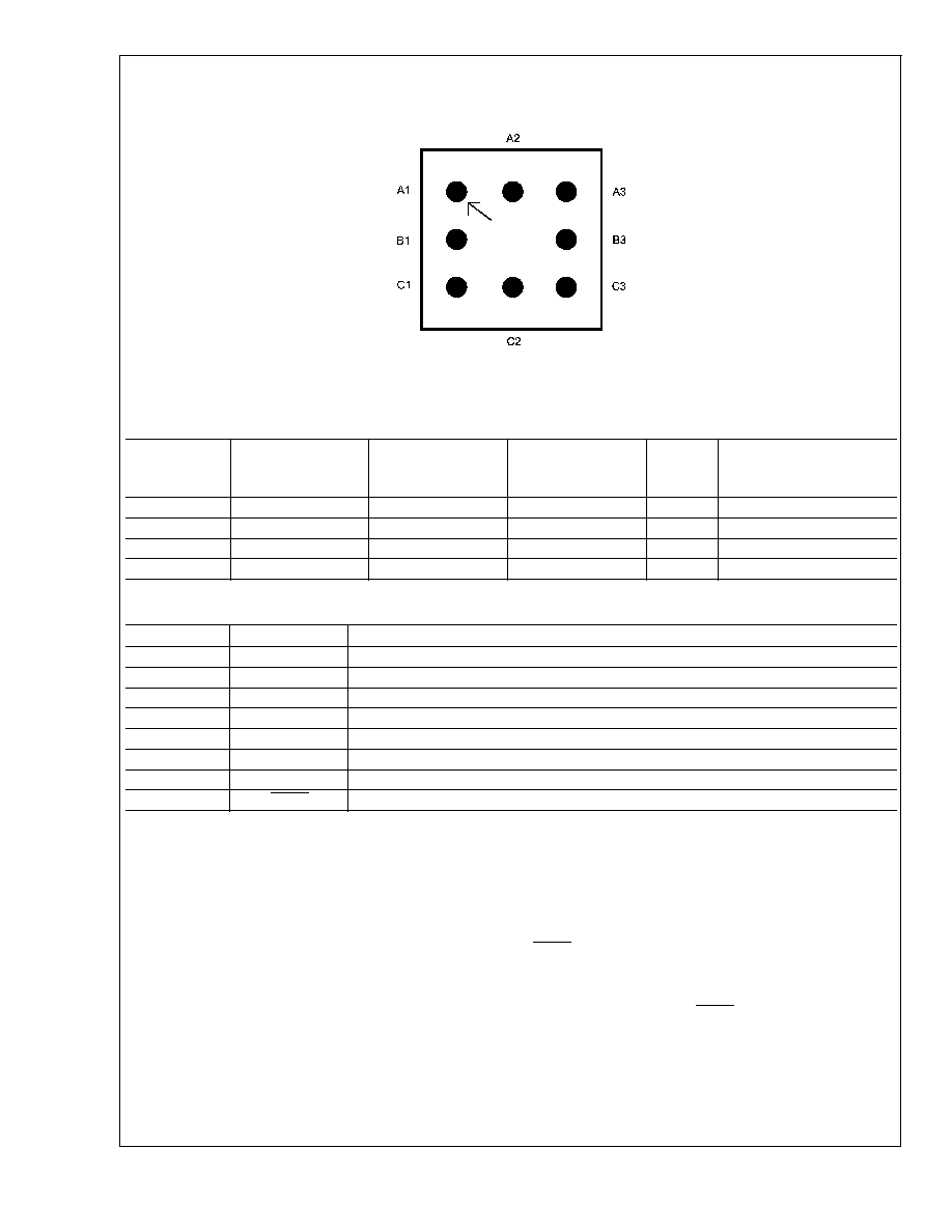
Connection Diagram
Top View
20065702
8-bump micro SMD
Ordering Information
Maximum
Output
Voltage
Order Number
Package Type
NSC Package
Drawing
Top Mark
Supplied As
16V
LM3500TL-16
micro SMD
TL08SSA
S18
250 Units, Tape and Reel
16V
LM3500TLX-16
micro SMD
TL08SSA
S18
3000 Units, Tape and Reel
21V
LM3500TL-21
micro SMD
TL08SSA
S23
250 Units, Tape and Reel
21V
LM3500TLX-21
micro SMD
TL08SSA
S23
3000 Units, Tape and Reel
Pin Description/Functions
Pin
Name
Function
A1
AGND
Analog ground.
B1
V
IN
Analog and Power supply input.
C1
V
OUT
PMOS source connection for synchronous rectification.
C2
V
SW
Switch pin. Drain connections of both NMOS and PMOS power devices.
C3
GND
Power Ground.
B3
FB
Output voltage feedback connection.
A3
NC
No internal connection made to this pin.
A2
SHDN
Shutdown control pin.
AGND(pin A1): Analog ground pin. The analog ground pin
should tie directly to the GND pin.
V
IN
(pin B1): Analog and Power supply pin. Bypass this pin
with a capacitor, as close to the device as possible, con-
nected between the V
IN
and GND pins.
V
OUT
(pin C1): Source connection of internal PMOS power
device. Connect the output capacitor between the V
OUT
and
GND pins as close as possible to the device.
V
SW
(pin C2): Drain connection of internal NMOS and PMOS
switch devices. Keep the inductor connection close to this
pin to minimize EMI radiation.
GND(pin C3): Power ground pin. Tie directly to ground
plane.
FB(pin B3): Output voltage feedback connection. Set the
primary White LED network current with a resistor from the
FB pin to GND. Keep the current setting resistor close to the
device and connected between the FB and GND pins.
NC(pin A3): No internal connection is made to this pin. The
maximum allowable voltage that can be applied to this pin is
7.5V.
SHDN(pin A2): Shutdown control pin. Disable the device
with a voltage less than 0.3V and enable the device with a
voltage greater than 1.1V. The white LED current can be
controlled using a PWM signal at this pin. There is an
internal pull down on the SHDN pin, the device is in a
normally off state.
LM3500
www.national.com
2
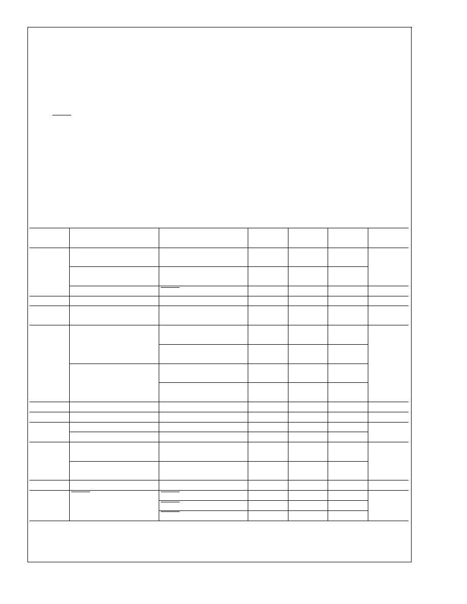
Absolute Maximum Ratings
(Note 1)
If Military/Aerospace specified devices are required,
please contact the National Semiconductor Sales Office/
Distributors for availability and specifications.
V
IN
-0.3V to 7.5V
V
OUT
(LM3500-16)(Note 2)
-0.3V to 16V
V
OUT
(LM3500-21)(Note 2)
-0.3V to 21V
V
SW
(Note 2)
-0.3V to V
OUT
+0.3V
FB, SHDN, and NC Voltages
-0.3V to 7.5V
Maximum Junction Temperature
150∞C
Lead Temperature
(Note 3)
300∞C
ESD Ratings (Note 4)
Human Body Model
2kV
Machine Model
200V
Operating Conditions
Ambient Temperature
(Note 5)
-40∞C to +85∞C
Junction Temperature
-40∞C to +125∞C
Supply Voltage
2.7V to 7V
Thermal Properties
Junction to Ambient Thermal
Resistance (
JA
)(Note 6)
75∞C/W
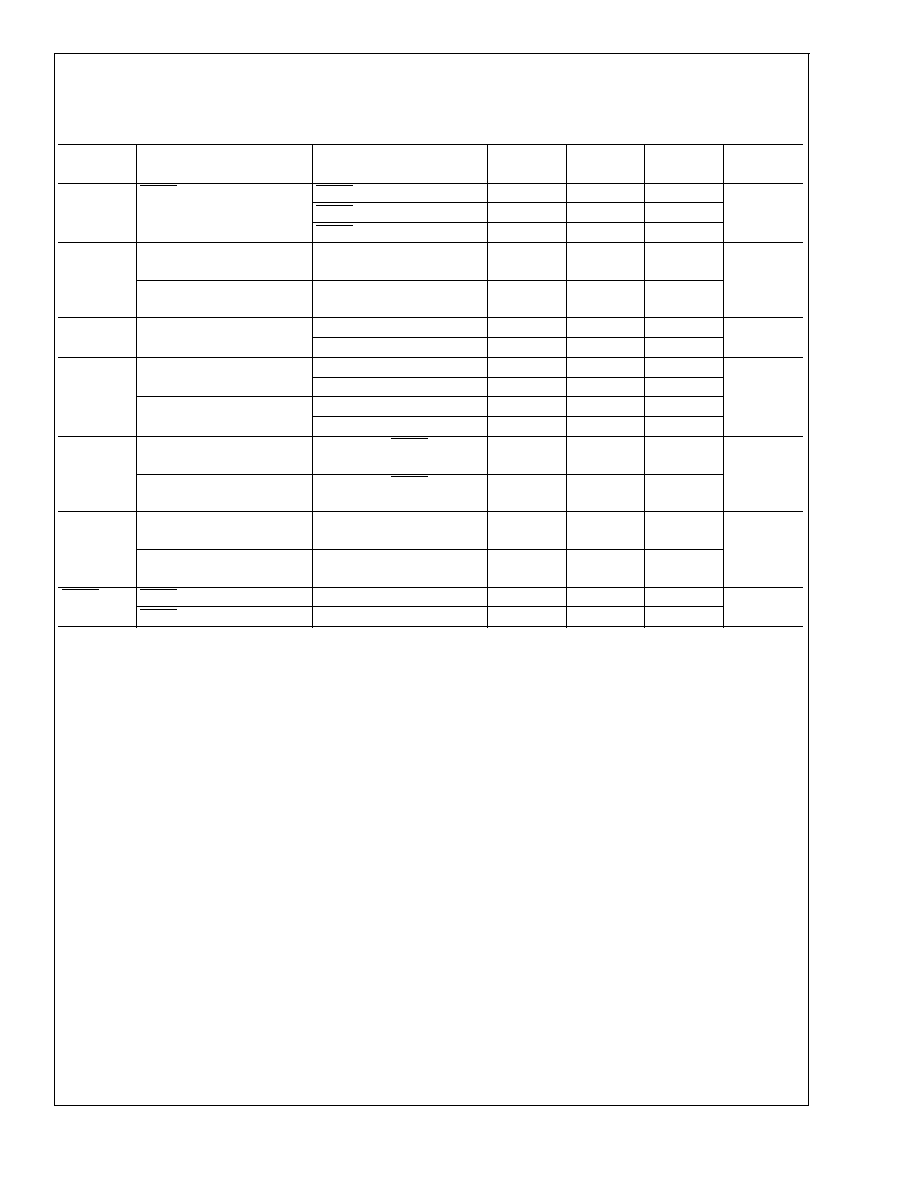
Electrical Characteristics
Specifications in standard type face are for T
A
= 25∞C and those in boldface type apply over the Operating Temperature
Range of T
A
= -10∞C to +85∞C. Unless otherwise specified V
IN
=2.7V and specification apply to both LM3500-16 and LM3500-
21.
Symbol
Parameter
Conditions
Min
(Note 7)
Typ
(Note 8)
Max
(Note 7)
Units
I
Q
Quiescent Current, Device
Not Switching
FB
>
0.54V
0.95
1.2
mA
Quiescent Current, Device
Switching
FB = 0V
1.8
2.5
Shutdown
SHDN = 0V
0.1
2
µA
V
FB
Feedback Voltage
V
IN
= 2.7V to 7V
0.47
0.5
0.53
V
V
FB
Feedback Voltage Line
Regulation
V
IN
= 2.7V to 7V
0.1
0.4
%/V
I
CL
Switch Current Limit
(LM3500-16)
V
IN
= 2.7V,
Duty Cycle = 80%
275
400
480
mA
V
IN
= 3.0V,
Duty Cycle = 70%
255
400
530
Switch Current Limit
(LM3500-21)
V
IN
= 2.7V,
Duty Cycle = 70%
420
640
770
V
IN
= 3.0V,
Duty Cycle = 63%
450
670
800
I
B
FB Pin Bias Current
FB = 0.5V (Note 9)
45
200
nA
V
IN
Input Voltage Range
2.7
7.0
V
R
DSON
NMOS Switch R
DSON
V
IN
= 2.7V, I
SW
= 300mA
0.43
PMOS Switch R
DSON
V
OUT
= 6V, I
SW
= 300mA
1.1
2.3
D
Limit
Duty Cycle Limit
(LM3500-16)
FB = 0V
80
87
%
Duty Cycle Limit
(LM3500-21)
FB = 0V
85
94
F
SW
Switching Frequency
0.85
1.0
1.15
MHz
I
SD
SHDN Pin Current (Note 10)
SHDN = 5.5V
18
30
µA
SHDN = 2.7V
9
16
SHDN = GND
0.1
LM3500
www.national.com
3
Electrical Characteristics
(Continued)
Specifications in standard type face are for T
A
= 25∞C and those in boldface type apply over the Operating Temperature
Range of T
A
= -10∞C to +85∞C. Unless otherwise specified V
IN
=2.7V and specification apply to both LM3500-16 and LM3500-
21.
Symbol
Parameter
Conditions
Min
(Note 7)
Typ
(Note 8)
Max
(Note 7)
Units
I
L
Switch Leakage Current
(LM3500-16)
V
SW
= 15V
0.01
0.5
µA
Switch Leakage Current
(LM3500-21)
V
SW
= 20V
0.01
2.0
UVP
Input Undervoltage Lockout
ON Threshold
2.4
2.5
2.6
V
OFF Threshold
2.3
2.4
2.5
OVP
Output Overvoltage
Protection (LM3500-16)
ON Threshold
15
15.5
16
V
OFF Threshold
14
14.6
15
Output Overvoltage
Protection (LM3500-21)
ON Threshold
20
20.5
21
OFF Threshold
19
19.5
20
I
Vout
V
OUT
Bias Current
(LM3500-16)
V
OUT
= 15V, SHDN = V
IN
260
400
µA
V
OUT
Bias Current
(LM3500-21)
V
OUT
= 20V, SHDN = V
IN
300
460
I
VL
PMOS Switch Leakage
Current (LM3500-16)
V
OUT
= 15V, V
SW
= 0V
0.01
3
µA
PMOS Switch Leakage
Current (LM3500-21)
V
OUT
= 20V, V
SW
= 0V
0.01
3
SHDN
Threshold
SHDN Low
0.65
0.3
V
SHDN High
1.1
0.65
Specifications in standard type face are for T
J
= 25∞C and those in boldface type apply over the full Operating Temperature
Range (T
J
= -40∞C to +125∞C). Unless otherwise specified V
IN
=2.7V and specification apply to both LM3500-16 and LM3500-
21.
Symbol
Parameter
Conditions
Min
(Note 7)
Typ
(Note 8)
Max
(Note 7)
Units
I
Q
Quiescent Current, Device
Not Switching
FB
>
0.54V
0.95
1.2
mA
Quiescent Current, Device
Switching
FB = 0V
1.8
2.5
Shutdown
SHDN = 0V
0.1
2
µA
V
FB
Feedback Voltage
V
IN
= 2.7V to 7V
0.47
0.5
0.53
V
V
FB
Feedback Voltage Line
Regulation
V
IN
= 2.7V to 7V
0.1
0.4
%/V
I
CL
Switch Current Limit
(LM3500-16)
V
IN
= 3.0V, Duty Cycle =
70%
400
mA
Switch Current Limit
(LM3500-21)
V
IN
= 3.0V, Duty Cycle =
63%
670
I
B
FB Pin Bias Current
FB = 0.5V (Note 9)
45
200
nA
V
IN
Input Voltage Range
2.7
7.0
V
R
DSON
NMOS Switch R
DSON
V
IN
= 2.7V, I
SW
= 300mA
0.43
PMOS Switch R
DSON
V
OUT
= 6V, I
SW
= 300mA
1.1
2.3
D
Limit
Duty Cycle Limit
(LM3500-16)
FB = 0V
87
%
Duty Cycle Limit
(LM3500-21)
FB = 0V
94
F
SW
Switching Frequency
0.8
1.0
1.2
MHz
LM3500
www.national.com
4
Electrical Characteristics
(Continued)
Specifications in standard type face are for T
J
= 25∞C and those in boldface type apply over the full Operating Temperature
Range (T
J
= -40∞C to +125∞C). Unless otherwise specified V
IN
=2.7V and specification apply to both LM3500-16 and LM3500-
21.
Symbol
Parameter
Conditions
Min
(Note 7)
Typ
(Note 8)
Max
(Note 7)
Units
I
SD
SHDN Pin Current (Note 10)
SHDN = 5.5V
18
30
µA
SHDN = 2.7V
9
16
SHDN = GND
0.1
I
L
Switch Leakage Current
(LM3500-16)
V
SW
= 15V
0.01
0.5
µA
Switch Leakage Current
(LM3500-21)
V
SW
= 20V
0.01
2.0
UVP
Input Undervoltage Lockout
ON Threshold
2.4
2.5
2.6
V
OFF Threshold
2.3
2.4
2.5
OVP
Output Overvoltage
Protection (LM3500-16)
ON Threshold
15
15.5
16
V
OFF Threshold
14
14.6
15
Output Overvoltage
Protection (LM3500-21)
ON Threshold
20
20.5
21
OFF Threshold
19
19.5
20
I
Vout
V
OUT
Bias Current
(LM3500-16)
V
OUT
= 15V, SHDN = V
IN
260
400
µA
V
OUT
Bias Current
(LM3500-21)
V
OUT
= 20V, SHDN = V
IN
300
460
I
VL
PMOS Switch Leakage
Current (LM3500-16)
V
OUT
= 15V, V
SW
= 0V
0.01
3
µA
PMOS Switch Leakage
Current (LM3500-21)
V
OUT
= 20V, V
SW
= 0V
0.01
3
SHDN
Threshold
SHDN Low
0.65
0.3
V
SHDN High
1.1
0.65
Note 1: Absolute maximum ratings are limits beyond which damage to the device may occur. Operating Ratings are conditions for which the device is intended to
be functional, but device parameter specifications may not be guaranteed. For guaranteed specifications and test conditions, see the Electrical Characteristics.
Note 2: This condition applies if V
IN
<
V
OUT
. If V
IN
>
V
OUT
, a voltage greater than V
IN
+ 0.3V should not be applied to the V
OUT
or V
SW
pins.
Note 3: For more detailed soldering information and specifications, please refer to National Semiconductor Application Note 1112: Micro SMD Wafer Level Chip
Scale Package (AN-1112), available at www.national.com.
Note 4: The human body model is a 100 pF capacitor discharged through a 1.5 k
resistor into each pin. The machine model is a 200 pF capacitor discharged
directly into each pin.
Note 5: In applications where high power dissipation and/or poor package thermal resistance is present, the maximum ambient temperature may have to be
derated. Maximum ambient temperature (T
A-MAX
) is dependent on the maximum operating junction temperature (T
J-MAX-OP
= 125
o
C), the maximum power
dissipation of the device in the application (P
D-MAX
), and the junction-to ambient thermal resistance of the part/package in the application (
JA
), as given by the
following equation: T
A-MAX
= T
J-MAX-OP
≠ (
JA
x P
D-MAX
).
Note 6: Junction-to-ambient thermal resistance (
JA
) is highly application and board-layout dependent. The 75
o
C/W figure provided was measured on a 4-layer test
board conforming to JEDEC standards. In applications where high maximum power dissipation exists, special care must be paid to thermal dissipation issues when
designing the board layout.
Note 7: All limits guaranteed at room temperature (standard typeface) and at temperature extremes (bold typeface). All room temperature limits are production
tested, guaranteed through statistical analysis or guaranteed by design. All limits at temperature extremes are guaranteed via correlation using standard Statistical
Quality Control (SQC) methods. All limits are used to calculate Average Outgoing Quality Level (AOQL).
Note 8: Typical numbers are at 25∞C and represent the most likely norm.
Note 9: Feedback current flows out of the pin.
Note 10: Current flows into the pin.
LM3500
www.national.com
5
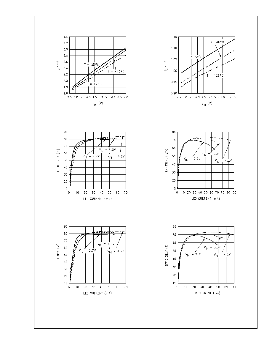
Typical Performance Characteristics
Switching Quiescent Current vs V
IN
Non-Switching Quiescent Current vs V
IN
20065755
20065756
2 LED Efficiency vs LED Current
L = Coilcraft DT1608C-223,
Efficiency = 100*(P
IN
/(2V
LED
*I
LED
))
2 LED Efficiency vs LED Current
L = TDK VLP4612T-220MR34,
Efficiency = 100*(P
IN
/(2V
LED
*I
LED
))
20065757
20065779
3 LED Efficiency vs LED Current
L = Coilcraft DT1608C-223,
Efficiency = 100*(P
IN
/(3V
LED
*I
LED
))
3 LED Efficiency vs LED Current
L = TDK VLP4612T-220MR34,
Efficiency = 100*(P
IN
/(3V
LED
*I
LED
))
20065758
20065780
LM3500
www.national.com
6
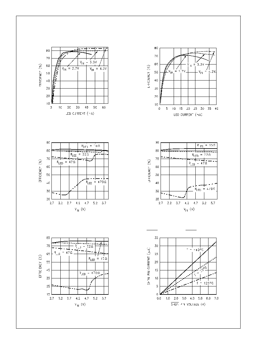
Typical Performance Characteristics
(Continued)
4 LED Efficiency vs LED Current
L = Coilcraft DT1608C-223,
Efficiency = 100*(P
IN
/(4V
LED
*I
LED
))
4 LED Efficiency vs LED Current
L = TDK VLP4612T-220MR34,
Efficiency = 100*(P
IN
/(4V
LED
*I
LED
))
20065759
20065781
2 LED Efficiency vs V
IN
L = Coilcraft DT1608C-223,
Efficiency = 100*(P
IN
/(2V
LED
*I
LED
))
3 LED Efficiency vs V
IN
L = Coilcraft DT1608C-223,
Efficiency = 100*(P
IN
/(3V
LED
*I
LED
))
20065769
20065770
4 LED Efficiency vs V
IN
L = Coilcraft DT1608C-223,
Efficiency = 100*(P
IN
/(4V
LED
*I
LED
))
SHDN Pin Current vs SHDN Pin Voltage
20065773
20065761
LM3500
www.national.com
7
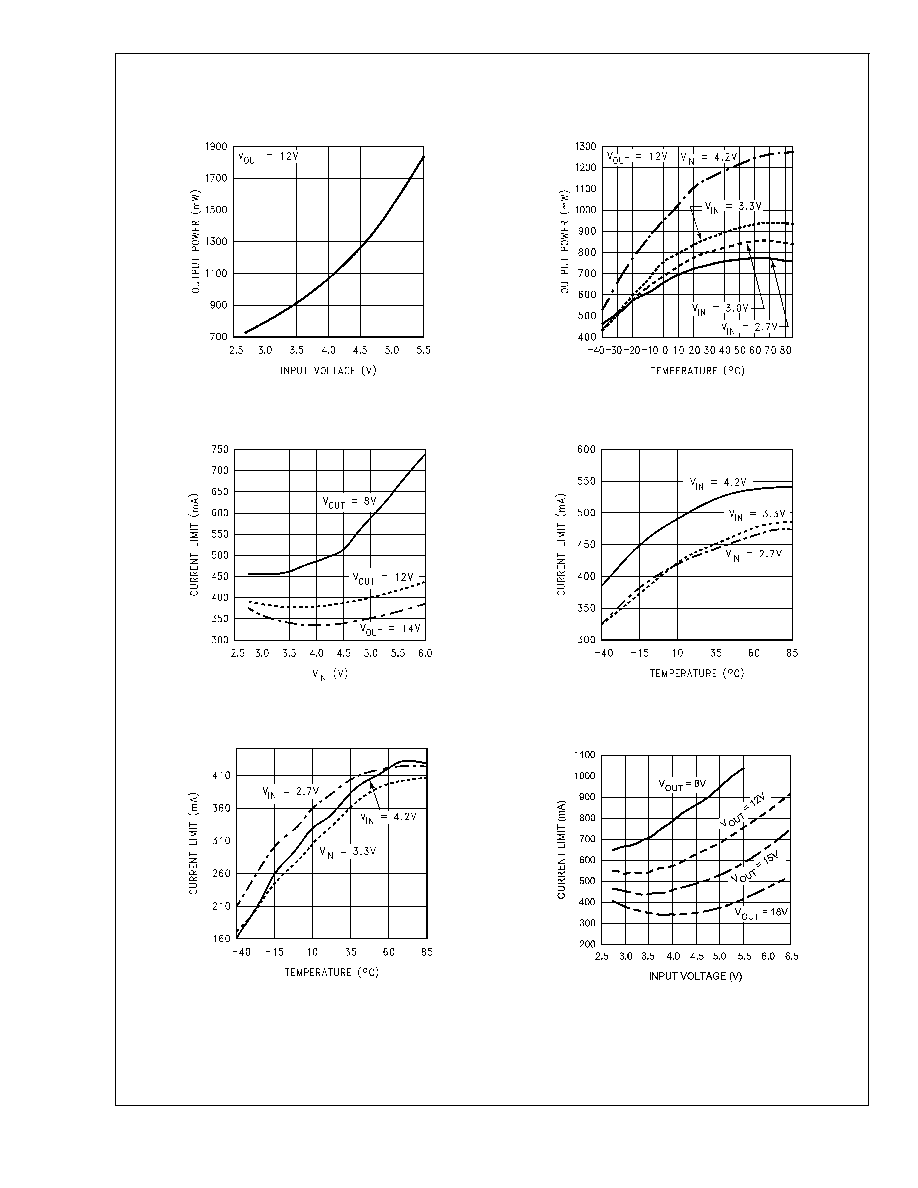
Typical Performance Characteristics
(Continued)
Output Power vs V
IN
: LM3500-16
(L = Coilcraft DT1608C-223)
Output Power vs Temperature: LM3500-16
(L = Coilcraft DT1608C-223)
20065784
20065785
Switch Current Limit vs V
IN
: LM3500-16
Switch Current Limit vs Temperature
LM3500-16, V
OUT
=8V
20065762
20065763
Switch Current Limit vs Temperature
LM3500-16, V
OUT
=12V
Switch Current Limit vs V
IN
: LM3500-21
20065776
20065791
LM3500
www.national.com
8

Typical Performance Characteristics
(Continued)
Switch Current Limit vs Temperature
LM3500-21, V
OUT
=8V
Switch Current Limit vs Temperature
LM3500-21, V
OUT
=12V
20065792
20065793
Switch Current Limit vs Temperature
LM3500-21, V
OUT
=18V
Oscillator Frequency vs V
IN
20065794
20065764
V
OUT
DC Bias vs V
OUT
Voltage: LM3500-16
V
OUT
DC Bias vs V
OUT
Voltage: LM3500-21
20065765
20065795
LM3500
www.national.com
9
Typical Performance Characteristics
(Continued)
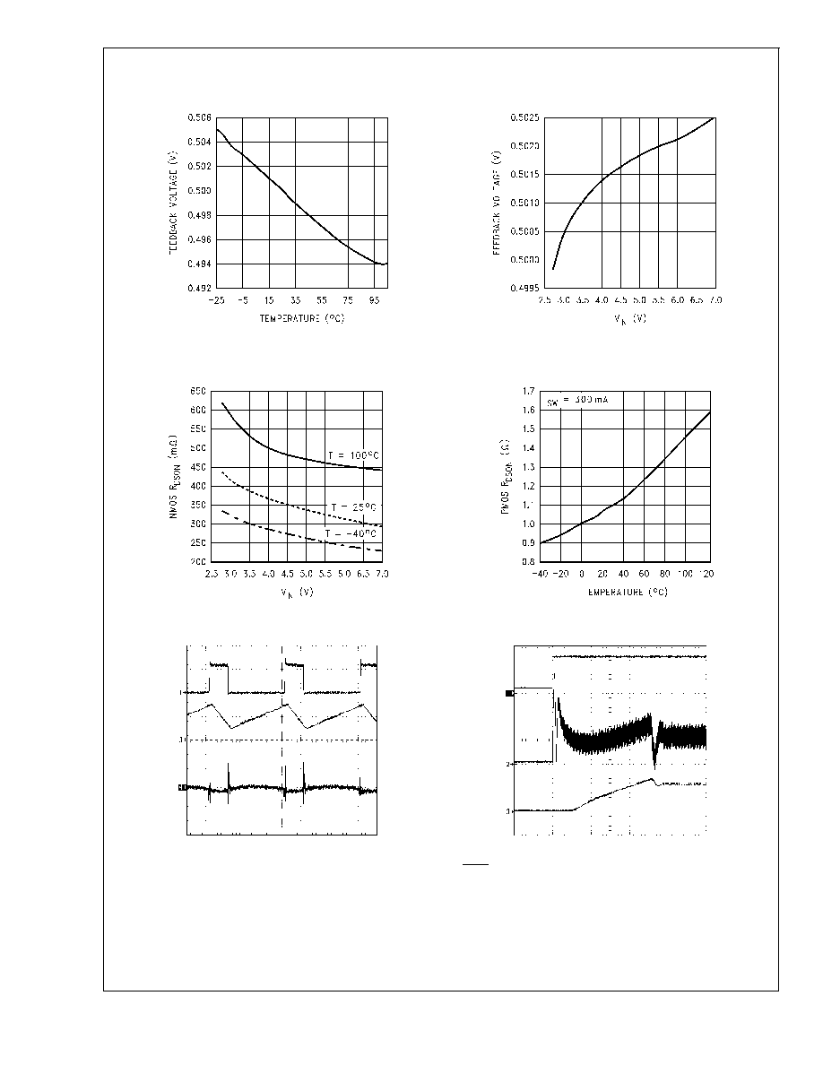
FB Voltage vs Temperature
FB Voltage vs V
IN
20065766
20065767
NMOS R
DSON
vs V
IN
(I
SW
= 300mA)
PMOS R
DSON
vs Temperature
20065774
20065775
Typical V
IN
Ripple
Start-Up: LM3500-16
20065768
LM3500-16, 3 LEDs, R
LED
= 22
, V
IN
= 3.0V
1) SW, 10V/div, DC
3) I
L
, 100mA/div, DC
4) V
IN
, 100mV/div, AC
T = 250ns/div
20065771
3 LEDs, R
LED
= 22
, V
IN
= 3.0V
1) SHDN, 1V/div, DC
2) I
L
, 100mA/div, DC
3) I
LED
, 20mA/div, DC
T = 100µs/div
LM3500
www.national.com
10
Typical Performance Characteristics
(Continued)
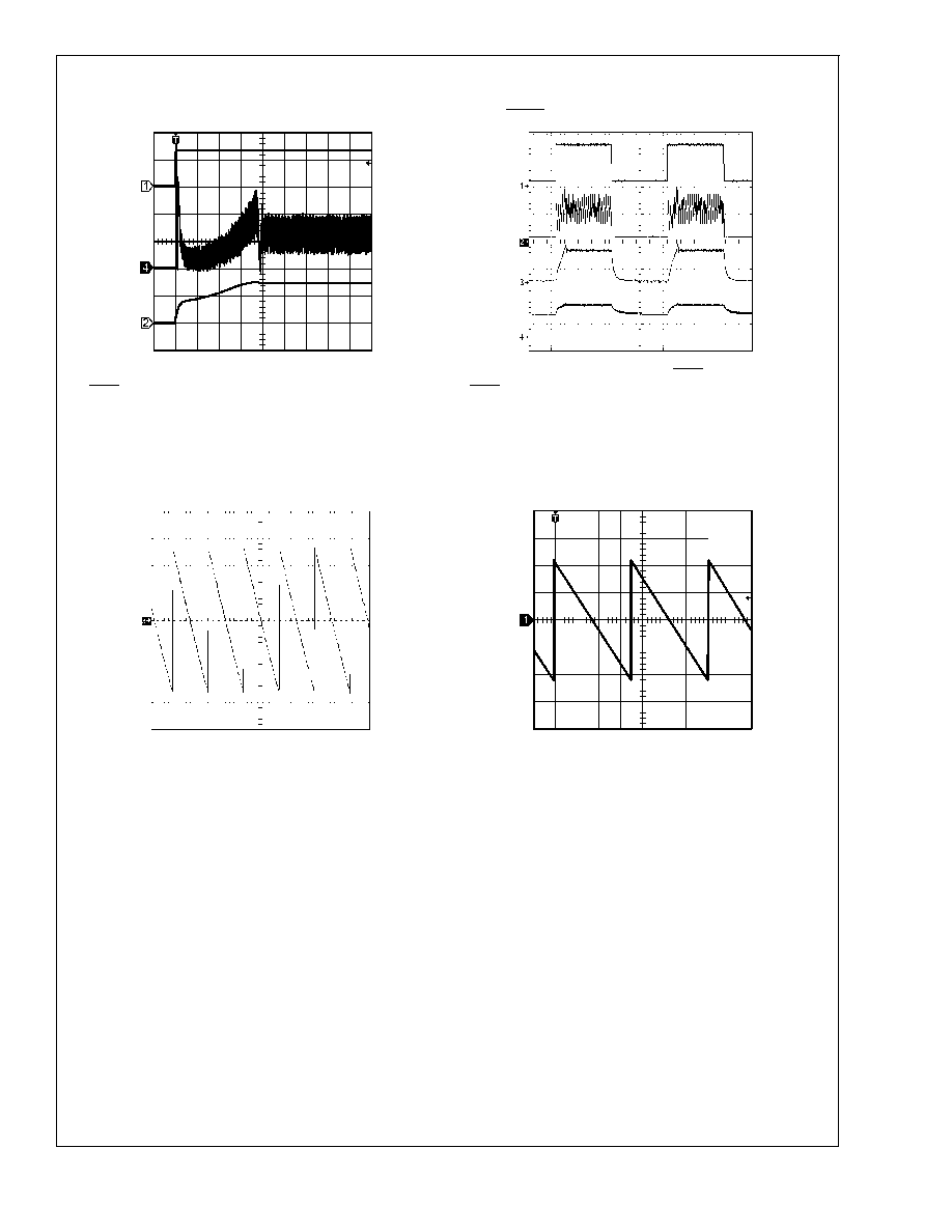
Start-Up: LM3500-21
SHDN Pin Duty Cycle Control Waveforms
20065796
3 LEDs, R
LED
= 22
, V
IN
= 3.0V
1) SHDN, 1V/div, DC
4) I
L
, 100mA/div, DC
2) V
OUT
, 10/div, DC
T = 200µs/div
V
CONT
= 2.7V
20065772
LM3500-16, 3 LEDs, R
LED
= 22
, V
IN
= 3.0V, SHDN frequency = 200Hz
1) SHDN, 1V/div, DC
2) I
L
, 100mA/div, DC
3) I
LED
, 20mA/div, DC
4) V
OUT
, 10V/div, DC
T = 1ms/div
Typical V
OUT
Ripple, OVP Functioning: LM3500-16
Typical V
OUT
Ripple, OVP Functioning: LM3500-21
20065782
V
OUT
open circuit and equals approximately 15V DC, V
IN
= 3.0V
3) V
OUT
, 200mV/div, AC
T = 1ms/div
20065797
V
OUT
open circuit and equals approximately 20V DC, V
IN
= 3.0V
1) V
OUT
, 200mV/div, AC
T = 400µs/div
LM3500
www.national.com
11
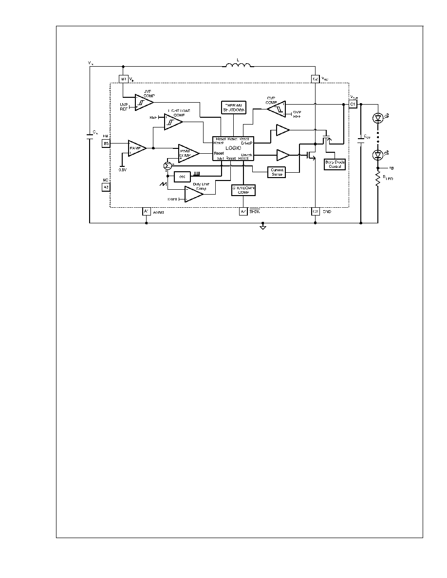
Operation
The LM3500 utilizes a synchronous Current Mode PWM
control scheme to regulate the feedback voltage over almost
all load conditions. The DC/DC controller acts as a controlled
current source ideal for white LED applications. The LM3500
is internally compensated preventing the use of any external
compensation components providing a compact overall so-
lution. The operation can best be understood referring to the
block diagram in Figure 1. At the start of each cycle, the
oscillator sets the driver logic and turns on the NMOS power
device conducting current through the inductor and turns off
the PMOS power device isolating the output from the V
SW
pin. The LED current is supplied by the output capacitor
when the NMOS power device is active. During this cycle,
the output voltage of the EAMP controls the current through
the inductor. This voltage will increase for larger loads and
decrease for smaller loads limiting the peak current in the
inductor minimizing EMI radiation. The EAMP voltage is
compared with a voltage ramp and the sensed switch volt-
age. Once this voltage reaches the EAMP output voltage,
the PWM COMP will then reset the logic turning off the
NMOS power device and turning on the PMOS power de-
vice. The inductor current then flows through the PMOS
power device to the white LED load and output capacitor.
The inductor current recharges the output capacitor and
supplies the current for the white LED branches. The oscil-
lator then sets the driver logic again repeating the process.
The Duty Limit Comp is always operational preventing the
NMOS power switch from being on more than one cycle and
conducting large amounts of current.
The LM3500 has dedicated protection circuitry active during
normal operation to protect the IC and the external compo-
nents. The Thermal Shutdown circuitry turns off both the
NMOS and PMOS power devices when the die temperature
reaches excessive levels. The LM3500 has a UVP Comp
that disables both the NMOS and PMOS power devices
when battery voltages are too low preventing an on state of
the power devices which could conduct large amounts of
current. The OVP Comp prevents the output voltage from
increasing beyond 15.5V(LM3500-16) and 20.5V(LM3500-
21) when the primary white LED network is removed or if
there is an LED failure, allowing the use of small (16V for
LM3500-16 and 25V for LM3500-21) ceramic capacitors at
the output. This comparator has hysteresis that will regulate
the output voltage between 15.5V and 14.6V typically for the
LM3500-16, and between 20.5V and 19.5V for the LM3500-
21. The LM3500 features a shutdown mode that reduces the
supply current to 0.1uA and isolates the input and output of
the converter.
20065704
FIGURE 1. LM3500 Block Diagram
LM3500
www.national.com
12
Application Information
ADJUSTING LED CURRENT
The White LED current is set using the following equation:
The LED current can be controlled using a PWM signal on
the SHDN pin with frequencies in the range of 100Hz
(greater than visible frequency spectrum) to 1kHz. For con-
trolling LED currents down to the µA levels, it is best to use
a PWM signal frequency between 200-500Hz. The LM3500
LED current can be controlled with PWM signal frequencies
above 1kHz but the controllable current decreases with
higher frequency. The maximum LED current would be
achieved using the equation above with 100% duty cycle, ie.
the SHDN pin always high.
LED-DRIVE CAPABILITY
The maximum number of LEDs that can be driven by the
LM3500 is limited by the output voltage capability of the
LM3500. When using the LM3500 in the typical application
configuration, with LEDs stacked in series between the V
OUT
and FB pins, the maximum number of LEDs that can be
placed in series (N
MAX
) is dependent on the maximum LED
forward voltage (V
F-MAX
), the voltage of the LM3500 feed-
back pin (V
FB-MAX
= 0.53V), and the minimum output over-
voltage protection level of the chosen LM3500 option
(LM3500-16: OVP
MIN
= 15V; LM3500-21: OVP
MIN
= 20V).
For the circuit to function properly, the following inequality
must be met:
(N
MAX
x V
F-MAX
) + 0.53V
OVP
MIN
When inserting a value for maximim LED V
F
, LED forward
voltage variation over the operating temperature range
should be considered. The table below provides maximum
LED voltage numbers for the LM3500-16 and LM3500-21 in
the typical application circuit configuration (with 3, 4, 5, 6, or
7 LEDs placed in series between the V
OUT
and FB pins).
# of LEDs
(in series)
Maximum LED V
F
LM3500-16
LM3500-21
3
4.82V
6.49V
4
3.61V
4.86V
5
2.89V
3.89V
6
X
3.24V
7
X
2.78V
For the LM3500 to operate properly, the output voltage must
be kept above the input voltage during operation. For most
applications, this requires a minimum of 2 LEDs (total of 6V
or more) between the FB and V
OUT
pins.
OUTPUT OVERVOLTAGE PROTECTION
The LM3500 contains dedicated circuitry for monitoring the
output voltage. In the event that the primary LED network is
disconnected from the LM3500-16, the output voltage will
increase and be limited to 15.5V (typ.). There is a 900mV
hysteresis associated with this circuitry which will cause the
output to fluctuate between 15.5V and 14.6V (typ.) if the
primary network is disconnected. In the event that the net-
work is reconnected regulation will begin at the appropriate
output voltage. The 15.5V limit allows the use of 16V 1µF
ceramic output capacitors creating an overall small solution
for white LED applications.
In the event that the primary LED network is disconnected
from the LM3500-21, the output voltage will increase and be
limited to 20.5V (typ.). There is a 1V hysteresis associated
with this circuitry which will cause the output to fluctuate
between 20.5V and 19.5V (typ.) if the primary network is
disconnected. In the event that the network is reconnected
regulation will begin at the appropriate output voltage. The
20.5V limit allows the use of 25V 1µF ceramic output capaci-
tors.
RELIABILITY AND THERMAL SHUTDOWN
The maximum continuous pin current for the 8 pin thin micro
SMD package is 535mA. When driving the device near its
power output limits the V
SW
pin can see a higher DC current
than 535mA (see INDUCTOR SELECTION section for aver-
age switch current). To preserve the long term reliability of
the device the average switch current should not exceed
535mA.
The LM3500 has an internal thermal shutdown function to
protect the die from excessive temperatures. The thermal
shutdown trip point is typically 150∞C. There is a hysteresis
of typically 35∞C so the die temperature must decrease to
approximately 115∞C before the LM3500 will return to normal
operation.
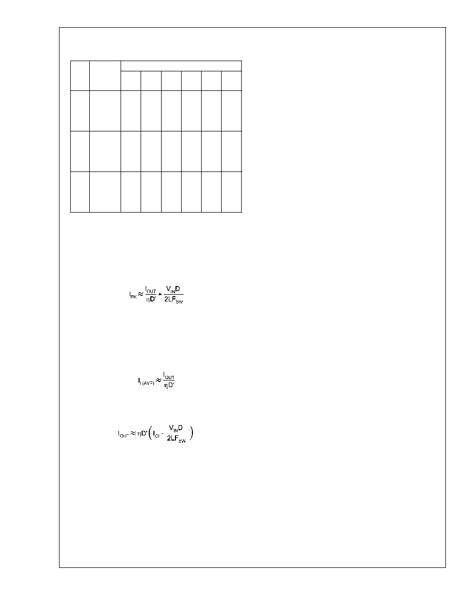
INDUCTOR SELECTION
The inductor used with the LM3500 must have a saturation
current greater than the cycle by cycle peak inductor current
(see Typical Peak Inductor Currents table below). Choosing
inductors with low DCR decreases power losses and in-
creases efficiency.
The minimum inductor value required for the LM3500-16 can
be calculated using the following equation:
The minimum inductor value required for the LM3500-21 can
be calculated using the following equation:
For both equations above, L is in µH, V
IN
is the input supply
of the chip in Volts, R
DSON
is the ON resistance of the NMOS
power switch found in the Typical Performance Characteris-
tics section in ohms and D is the duty cycle of the switching
regulator. The above equation is only valid for D greater than
or equal to 0.5. For applications where the minimum duty
cycle is less than 0.5, a 22µH inductor is the typical recom-
mendation for use with most applications. Bench-level veri-
fication of circuit performance is required in these special
cases, however. The duty cycle, D, is given by the following
equation:
where V
OUT
is the voltage at pin C1.
LM3500
www.national.com
13
Application Information
(Continued)
Typical Peak Inductor Currents (mA)
V
IN
(V)
# LEDs
(in
series)
LED Current
15
mA
20
mA
30
mA
40
mA
50
mA
60
mA
2.7
2
82
100
134
160
204
234
3
118
138
190
244
294
352
4
142
174
244
322
X
X
5
191
232
319
413
X
X
3.3
2
76
90
116
136
172
198
3
110
126
168
210
250
290
4
132
158
212
270
320
X
5
183
216
288
365
446
X
4.2
2
64
76
96
116
142
162
3
102
116
148
180
210
246
4
122
146
186
232
272
318
5
179
206
263
324
388
456
C
IN
= C
OUT
= 1 µF
L = 22 µH, 160 m
DCR max. Coilcraft DT1608C-223
2 and 3 LED applications: LM3500-16 or LM3500-21; LED V
F
= 3.77V at
20mA; T
A
= 25∞C
4 LED applications: LM3500-16 or LM3500-21; LED V
F
= 3.41V at 20mA; T
A
= 25∞C
5 LED applications: LM3500-21 only; LED V
F
= 3.28V at 20mA; T
A
= 25∞C
The typical cycle-by-cycle peak inductor current can be cal-
culated from the following equation:
where I
OUT
is the total load current, F
SW
is the switching
frequency, L is the inductance and
is the converter effi-
ciency of the total driven load. A good typical number to use
for
is 0.8. The value of can vary with load and duty cycle.
The average inductor current, which is also the average V
SW
pin current, is given by the following equation:
The maximum output current capability of the LM3500 can
be estimated with the following equation:
where I
CL
is the current limit. Some recommended inductors
include but are not limited to:
Coilcraft DT1608C series
Coilcraft DO1608C series
TDK VLP4612 series
TDK VLP5610 series
TDK VLF4012A series
CAPACITOR SELECTION
Choose low ESR ceramic capacitors for the output to mini-
mize output voltage ripple. Multilayer X7R or X5R type ce-
ramic capacitors are the best choice. For most applications,
a 1µF ceramic output capacitor is sufficient.
Local bypassing for the input is needed on the LM3500.
Multilayer X7R or X5R ceramic capacitors with low ESR are
a good choice for this as well. A 1µF ceramic capacitor is
sufficient for most applications. However, for some applica-
tions at least a 4.7µF ceramic capacitor may be required for
proper startup of the LM3500. Using capacitors with low
ESR decreases input voltage ripple. For additional bypass-
ing, a 100nF ceramic capacitor can be used to shunt high
frequency ripple on the input. Some recommended capaci-
tors include but are not limited to:
TDK C2012X7R1C105K
Taiyo-Yuden EMK212BJ105 G
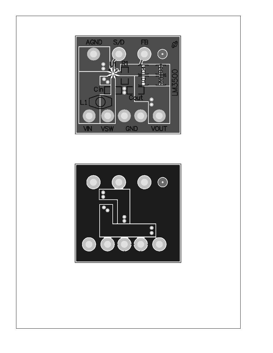
LAYOUT CONSIDERATIONS
The input bypass capacitor C
IN
, as shown in Figure 1, must
be placed close to the device and connect between the V
IN
and GND pins. This will reduce copper trace resistance
which effects the input voltage ripple of the IC. For additional
input voltage filtering, a 100nF bypass capacitor can be
placed in parallel with C
IN
to shunt any high frequency noise
to ground. The output capacitor, C
OUT
, should also be placed
close to the LM3500 and connected directly between the
V
OUT
and GND pins. Any copper trace connections for the
C
OUT
capacitor can increase the series resistance, which
directly effects output voltage ripple and efficiency. The cur-
rent setting resistor, R
LED
, should be kept close to the FB pin
to minimize copper trace connections that can inject noise
into the system. The ground connection for the current set-
ting resistor should connect directly to the GND pin. The
AGND pin should connect directly to the GND pin. Not
connecting the AGND pin directly, as close to the chip as
possible, may affect the performance of the LM3500 and
limit its current driving capability. Trace connections made to
the inductor should be minimized to reduce power dissipa-
tion, EMI radiation and increase overall efficiency. It is good
practice to keep the V
SW
routing away from sensitive pins
such as the FB pin. Failure to do so may inject noise into the
FB pin and affect the regulation of the device. See Figure 2
and Figure 3 for an example of a good layout as used for the
LM3500 evaluation board.
LM3500
www.national.com
14
Application Information
(Continued)
20065777
FIGURE 2. Evaluation Board Layout (2X Magnification)
Top Layer
20065778
FIGURE 3. Evaluation Board Layout (2X Magnification)
Bottom Layer (as viewed from the top)
LM3500
www.national.com
15
Application Information
(Continued)
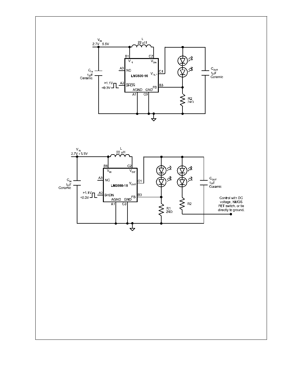
20065709
FIGURE 4. 2 White LED Application
20065754
FIGURE 5. Multiple 2 LED String Application
LM3500
www.national.com
16
Application Information
(Continued)
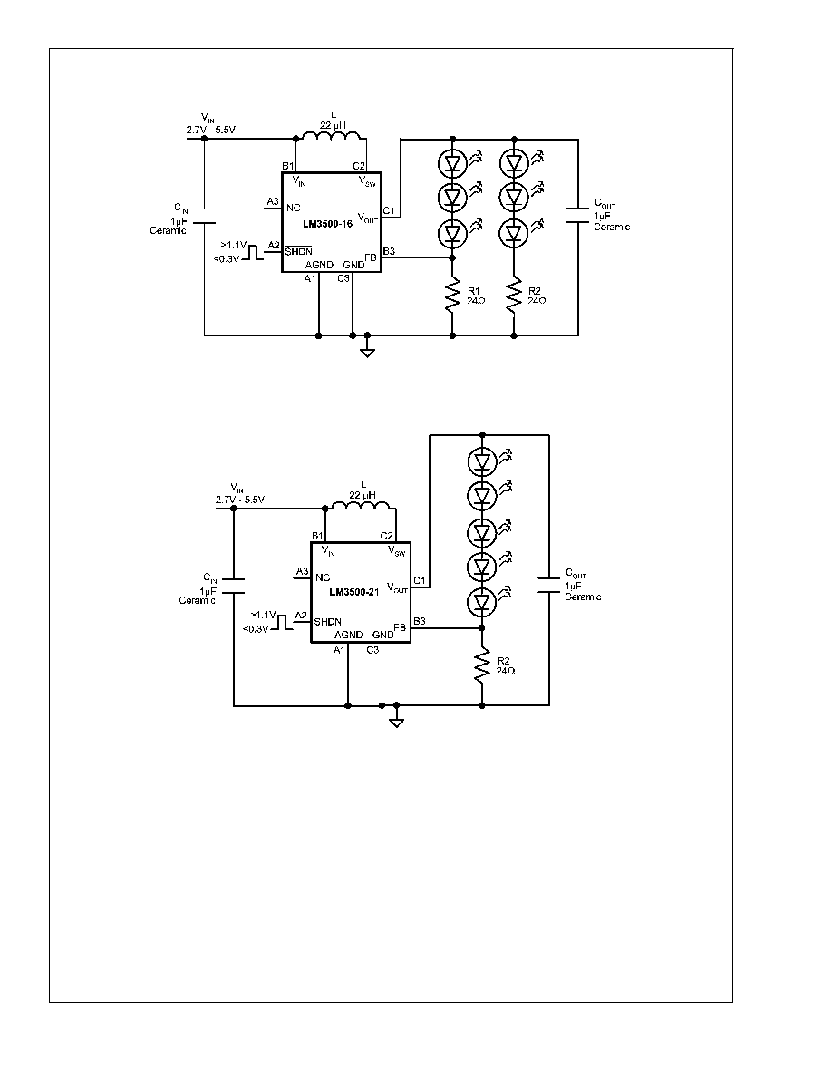
20065783
FIGURE 6. Multiple 3 LED String Application
20065790
FIGURE 7. LM3500-21 5 LED Application
LM3500
www.national.com
17
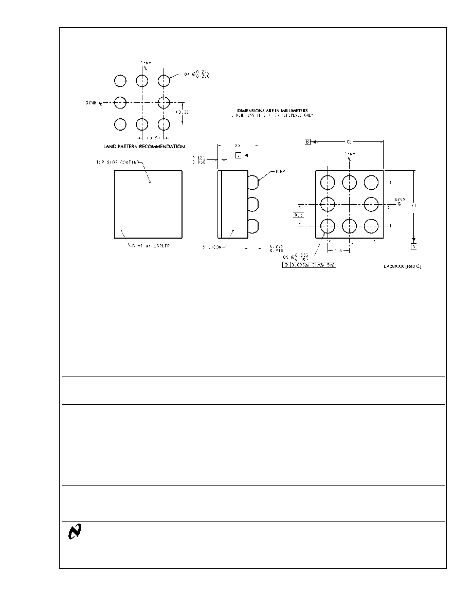
Physical Dimensions
inches (millimeters)
unless otherwise noted
8-Bump Micro SMD Package (TL)
For Ordering, Refer to Ordering Information Table
NS Package Number TLA08SSA
X1 = 1.92mm (
±
0.03mm), X2 = 1.92mm (
±
0.03mm), X3 = 0.6mm (
±
0.075mm)
National does not assume any responsibility for use of any circuitry described, no circuit patent licenses are implied and National reserves
the right at any time without notice to change said circuitry and specifications.
For the most current product information visit us at www.national.com.
LIFE SUPPORT POLICY
NATIONAL'S PRODUCTS ARE NOT AUTHORIZED FOR USE AS CRITICAL COMPONENTS IN LIFE SUPPORT DEVICES OR SYSTEMS
WITHOUT THE EXPRESS WRITTEN APPROVAL OF THE PRESIDENT AND GENERAL COUNSEL OF NATIONAL SEMICONDUCTOR
CORPORATION. As used herein:
1. Life support devices or systems are devices or systems
which, (a) are intended for surgical implant into the body, or
(b) support or sustain life, and whose failure to perform when
properly used in accordance with instructions for use
provided in the labeling, can be reasonably expected to result
in a significant injury to the user.
2. A critical component is any component of a life support
device or system whose failure to perform can be reasonably
expected to cause the failure of the life support device or
system, or to affect its safety or effectiveness.
BANNED SUBSTANCE COMPLIANCE
National Semiconductor manufactures products and uses packing materials that meet the provisions of the Customer Products
Stewardship Specification (CSP-9-111C2) and the Banned Substances and Materials of Interest Specification (CSP-9-111S2) and contain
no ``Banned Substances'' as defined in CSP-9-111S2.
National Semiconductor
Americas Customer
Support Center
Email: new.feedback@nsc.com
Tel: 1-800-272-9959
National Semiconductor
Europe Customer Support Center
Fax: +49 (0) 180-530 85 86
Email: europe.support@nsc.com
Deutsch Tel: +49 (0) 69 9508 6208
English
Tel: +44 (0) 870 24 0 2171
FranÁais Tel: +33 (0) 1 41 91 8790
National Semiconductor
Asia Pacific Customer
Support Center
Email: ap.support@nsc.com
National Semiconductor
Japan Customer Support Center
Fax: 81-3-5639-7507
Email: jpn.feedback@nsc.com
Tel: 81-3-5639-7560
www.national.com
Synchronous
Step-up
DC/DC
Converter
for
White
LED
Applications