
LM3503
Dual-Display Constant Current LED Driver with Analog
Brightness Control
General Description
The LM3503 is a white LED driver for lighting applications.
For dual display backlighting applications, the LM3503 pro-
vides a complete solution. The LM3503 contains two internal
white LED current bypass FET (Field Effect Transistor)
switches. The white LED current can be adjusted with a DC
voltage from a digital to analog converter or RC filtered PWM
(pulse-width-modulated) signal at the Cntrl pin.
With no external compensation, cycle-by-cycle current limit,
output over-voltage protection, input under-voltage protec-
tion, and dynamic white LED current control capability, the
LM3503 offers superior performance over other step-up
white LED drivers.
Features
n
Drives up to 4, 6, 8 or 10 White LEDs for Dual Display
Backlighting
n
>
80% Peak Efficiency
n
Output Voltage Protection Options: 16V, 25V, 35V & 44V
n
Input Under-Voltage Protection
n
Internal Soft Start Eliminates Inrush Current
n
1 MHz Constant-Switching Frequency
n
Analog Brightness Control
n
Wide Input Voltage Range: 2.5V to 5.5V
n
Low Profile Packages:
<
1 mm Height
-- 10 Bump MicroSMD
-- 16 Pin LLP
Applications
n
Dual-Display Display Backlighting in Portable devices
n
Cellular Phones and PDAs
Typical Application
20128662
July 2005
LM3503
Dual-Display
Constant
Current
LED
Driver
with
Analog
Brightness
Control
© 2005 National Semiconductor Corporation
DS201286
www.national.com
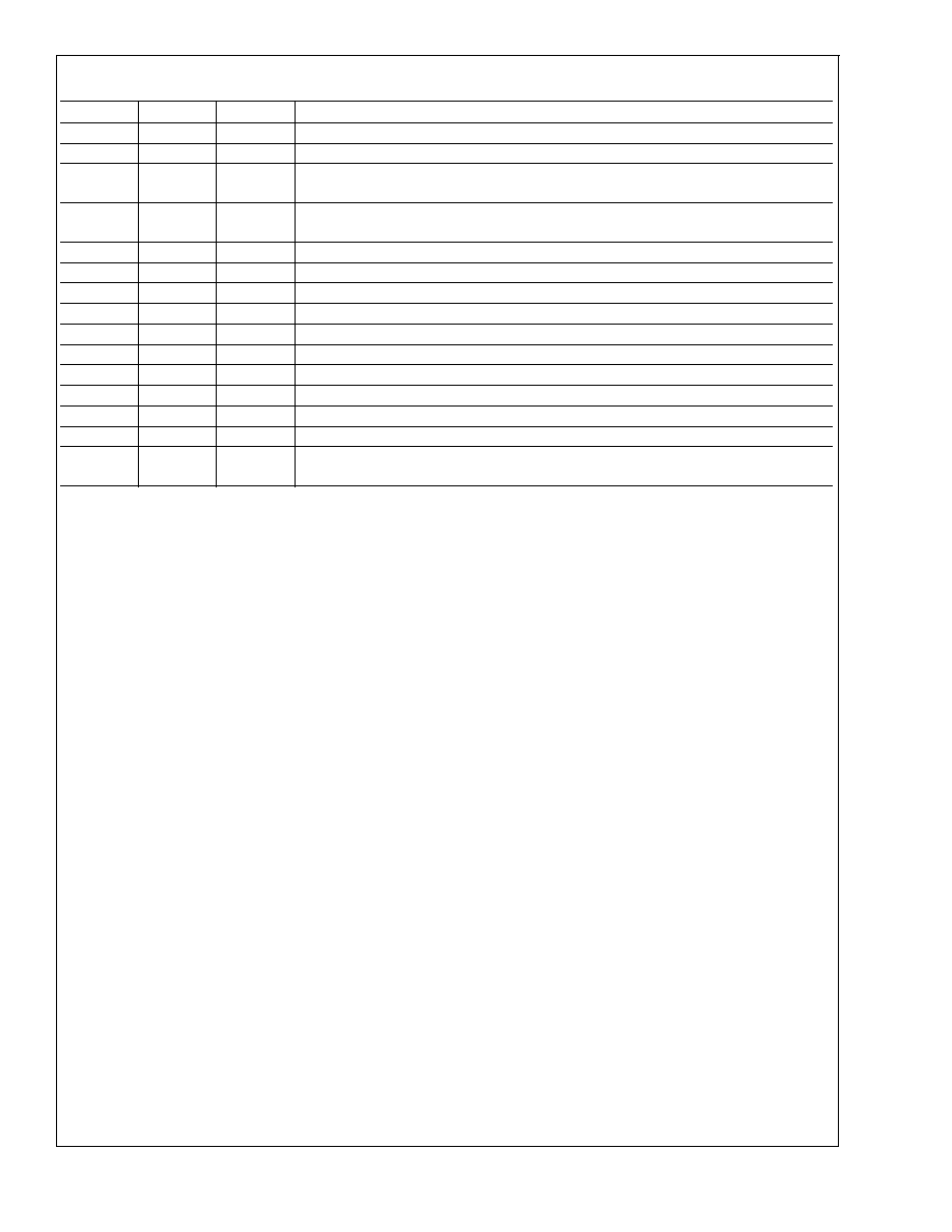
Pin Descriptions/Functions
Bump #
Pin #
Name
Description
A1
9
Cntrl
White LED Current Control Connection
B1
7
Fb
Feedback Voltage Connection
C1
6
V
OUT2
Drain Connections of the NMOS and PMOS Field Effect Transistor (FET) Switches
(Figure 1: N2 and P1). Connect 100nF at V
OUT2
node if V
OUT2
is not used
D1
4
V
OUT1
Over-Voltage Protection (OVP) and Source Connection of the PMOS FET Switch
(Figure 1: P1)
D2
2 and 3
Sw
Drain Connection of the Power NMOS Switch (Figure 1: N1)
D3
15 and 16
Pgnd
Power Ground Connection
C3
14
Agnd
Analog Ground Connection
B3
13
V
IN
Input Voltage Connection
A3
12
En2
NMOS FET Switch Control Connection
A2
10
En1
PMOS FET Switch Control Connection
1
NC
No Connection
5
NC
No Connection
8
NC
No Connection
11
NC
No Connection
DAP
DAP
Die Attach Pad (DAP), to be soldered to the printed circuit board's ground plane for
enhanced thermal dissipation.
Cntrl (Bump A1): White LED current control pin. Use this
pin to control the feedback voltage with an external DC
voltage. The feedback voltage is given as V
Fb
= (0.156) *
(V
Cntrl
) for the control voltage range of 0V
V
Cntrl
3.5V.
Fb (Bump B1):Output voltage feedback connection.
V
OUT2
(Bump C1):Drain connections of the internal PMOS
and NMOS FET switches (Figure 1: P1 and N2). It is recom-
mended to connect 100nF at V
OUT2
if V
OUT2
is not used for
LM3503-35V & LM3503-44V versions.
V
OUT1
(Bump D1):
Source connection of the internal PMOS FET switch (Figure
1: P1) and OVP sensing node. The output capacitor must be
connected as close to the device as possible, between the
V
OUT1
pin and ground plane. Also connect the Schottky
diode as close as possible to the V
OUT1
pin to minimize trace
resistance and EMI radiation.
Sw (Bump D2):
Drain connection of the internal power NMOS FET switch
(Figure 1: N1). Minimize the metal trace length and maxi-
mize the metal trace width connected to this pin to reduce
EMI radiation and trace resistance.
Pgnd (Bump D3): Power ground pin. Connect directly to the
ground plane.
Agnd (Bump C3):Analog ground pin. Connect the analog
ground pin directly to the Pgnd pin.
V
IN
(Bump B3): Input voltage connection pin. The C
IN
ca-
pacitor should be as close to the device as possible, be-
tween the V
IN
pin and ground plane.
En2 (Bump A3): Enable pin for the internal NMOS FET
switch (Figure 1: N2) during device operation. When V
En2
is
1.4V, the internal NMOS FET switch turns off and the SUB
display is turned on. The En2 pin has an internal pull down
circuit, thus the internal NMOS FET switch is normally in the
on state of operation with the SUB display turned off. When
V
En2
is
0.3V, the internal NMOS FET switch turns on and
the SUB display is turned off. If both V
En1
and V
En2
are
0.3V the LM3503 will shutdown. If V
OUT2
is not used, En2
must be floating or grounded and En1 used to enable the
device.
En1 (Bump A2): Enable pin for the internal PMOS FET
switch (Figure 1: P1) during device operation. When V
En1
is
0.3V, the internal PMOS FET switch turns on and the MAIN
display is turned off. When V
En1
is
1.4V, the internal PMOS
FET switch turns off and the MAIN display is turned on. If
both V
En1
and V
En2
are
0.3V the LM3503 will shutdown.
The En1 pin has an internal pull down circuit, thus the
internal PMOS FET switch is normally in the on state of
operation with the MAIN display turned off. If V
OUT2
is not
used, En2 must be grounded and En1 use to enable the
device.
LM3503
www.national.com
3

Ordering Information
Voltage
Option
Order Number
Package
Marking
Supplied As
16
LM3503ITL-16
SBHB
250 Units, Tape-and-Reel
16
LM3503ITLX-16
SBHB
3000 Units, Tape-and-Reel
16
LM3503SQ-16
L00045B
1000 Units, Tape-and-Reel
16
LM3503SQX-16
L00045B
4500 Units, Tape-and-Reel
25
LM3503ITL-25
SBJB
250 Units, Tape-and-Reel
25
LM3503ITLX-25
SBJB
3000 Units, Tape-and-Reel
25
LM3503SQ-25
L00046B
1000 Units, Tape-and-Reel
25
LM3503SQX-25
L00046B
4500 Units, Tape-and-Reel
35
LM3503ITL-35
SBKB
250 Units, Tape-and-Reel
35
LM3503ITLX-35
SBKB
3000 Units, Tape-and-Reel
35
LM3503SQ-35
L00047B
1000 Units, Tape-and-Reel
35
LM3503SQX-35
L00047B
4500 Units, Tape-and-Reel
44
LM3503ITL-44
SDNB
250 Units, Tape-and-Reel
44
LM3503ITLX-44
SDNB
3000 Units, Tape-and-Reel
44
LM3503SQ-44
L00053B
1000 Units, Tape-and-Reel
44
LM3503SQX-44
L00053B
4500 Units, Tape-and-Reel
LM3503
www.national.com
4
Absolute Maximum Ratings
(Note 1)
If Military/Aerospace specified devices are required,
please contact the National Semiconductor Sales Office/
Distributors for availability and specifications.
V
IN
Pin
-0.3V to +5.5V
Sw Pin
-0.3V to +48V
Fb Pin
-0.3V to +5.5V
Cntrl Pin
-0.3V to +5.5V
V
OUT1
Pin
-0.3V to +48V
V
OUT2
Pin
-0.3V to V
OUT1
En1
-0.3V to +5.5V
En2
-0.3V to +5.5V
Continuous Power Dissipation
Internally Limited
Maximum Junction Temperature
(T
J-MAX
)
+150∞C
Storage Temperature Range
-65∞C to +150∞C
ESD Rating (Note 2)
Human Body Model:
Machine Model:
2 kV
200V
Operating Conditions
(Notes 1, 6)
Junction Temperature (T
J
) Range
-40∞C to +125∞C
Ambient Temperature (T
A
) Range
-40∞C to +85∞C
Supply Voltage, V
IN
Pin
2.5V to 5.5V
En1 and En2 Pins
0V to 5.5V
Cntrl Pin
0V to 3.5V
Thermal Properties
(Note 4)
Junction-to-Ambient Thermal Resistance (
JA
)
Micro SMD Package
65∞C/W
Leadless Leadframe Package
49∞C/W
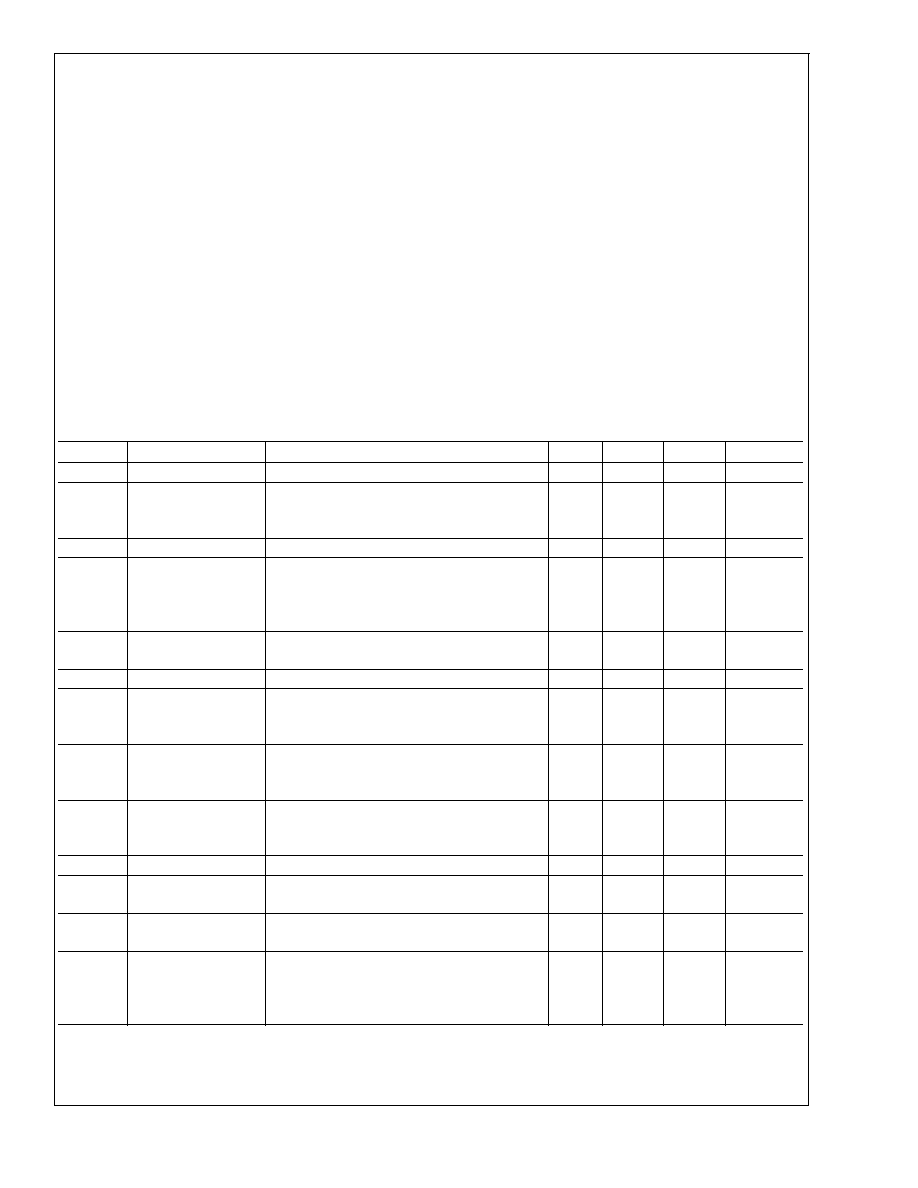
Electrical Characteristics
(Notes 6, 7) Limits in standard typeface are for T
J
= +25∞C. Limits in bold type-
face apply over the full operating junction temperature range (-40∞C
T
J
+125∞C). Unless otherwise specified,V
IN
= 2.5V.
Symbol
Parameter
Conditions
Min
Typ
Max
Units
V
IN
Input Voltage
2.5
5.5
V
I
Q
Non-Switching
Switching
Shutdown
Cntrl = 1.6V
Fb = 0V, Sw Is Floating
En1 = En2 = 0V
0.5
1.9
0.1
1
3
3
mA
mA
µA
V
Fb
Feedback Voltage
Cntrl = 3.5V
0.5
0.55
0.6
V
I
CL
NMOS Power Switch
Current Limit
16, Fb = 0V
25, Fb = 0V
35, Fb = 0V
44,FB = 0V
250
400
450
450
400
600
750
750
650
800
1050
1050
mA
I
Fb
Feedback Pin Output
Bias Current
Fb = 0.25V, Cntrl = 1.6V
64
500
nA
F
S
Switching Frequency
0.8
1
1.2
MHz
R
DS(ON)
NMOS Power Switch
ON Resistance
(Figure 1: N1)
I
Sw
= 500 mA, (Note 8)
0.55
1.1
R
PDS(ON)
PMOS ON Resistance
Of V
OUT1
/V
OUT2
Switch (Figure 1: P1)
I
PMOS
= 20 mA, En1 = 0V, En2 = 1.5V
5
10
R
NDS(ON)
NMOS ON Resistance
Of V
OUT2
/Fb Switch
(Figure 1: N2)
I
NMOS
= 20 mA, En1 = 1.5V, En2 = 0V
2.5
5
D
MAX
Maximum Duty Cycle
Fb = 0V
90
95
%
I
CNTRL
Cntrl Pin Bias Current
(Note 3)
Cntrl = 2.5V
Cntrl = 0V
8
0.1
14
µA
I
Sw
Sw Pin Leakage
Current (Note 3)
Sw = 42V, En1 = En2 =0V
0.01
5
µA
I
VOUT1(OFF)
V
OUT1
Pin Leakage
Current (Note 3)
V
OUT1
= 14V, En1 = En2 = 0V (16)
V
OUT1
= 23V, En1 = En2 = 0V (25)
V
OUT1
= 32V, En1 = En2 = 0V (35)
V
OUT1
= 42V, En1 = En2 = 0V (44)
0.1
0.1
0.1
0.1
3
3
3
3
µA
LM3503
www.national.com
5
