
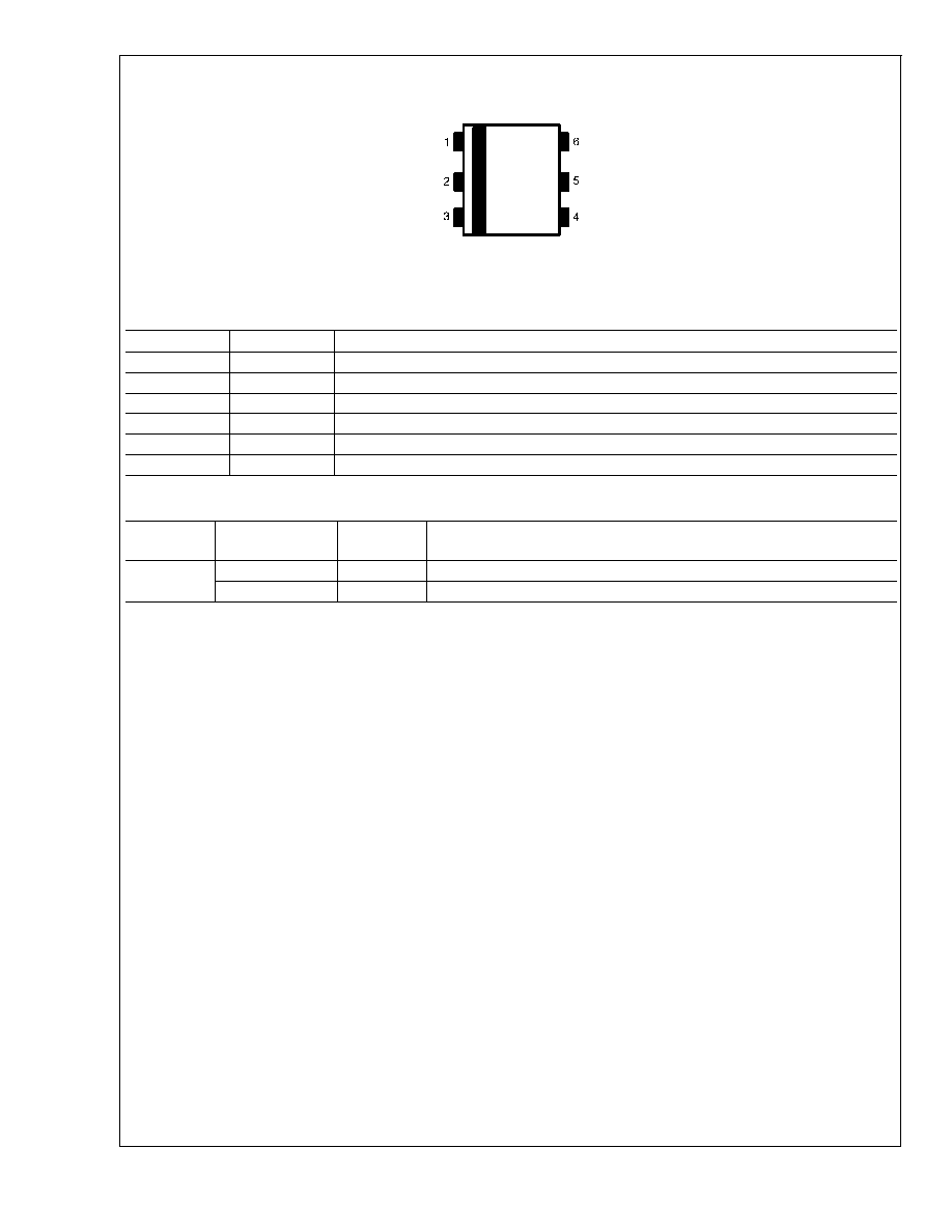
Connection Diagram
6-Lead SOT23 Package
20160202
Top View
Pin Descriptions
Pin #
Name
Description
1
En
Device Enable Connection
2
Gnd
Ground Connection
3
V
OUT
Output Voltage Connection
4
LED_rtn
White LED Current Sensing Input Connection
5
S
W
Drain Connection of the Internal Power Field Effect Transistor (FET) Switch
6
V
IN
Input or Supply Voltage Connection
Ordering Information
Current
Option
Order Number
Package
Marking
Supplied As
20 mA
LM3519MK-20
D52B
1000 Units, Tape-and-Reel
LM3519MKX-20
D52B
3000 Units, Tape-and-Reel
LM3519
www.national.com
2
Absolute Maximum Ratings
(Note 1)
If Military/Aerospace specified devices are required,
please contact the National Semiconductor Sales Office/
Distributors for availability and specifications.
V
IN
, En, & LED_rtn Pin
-0.3V to +6.5V
V
OUT
, Sw Pin
-0.3V to +21V
Maximum Junction Temperature
(T
J-MAX
)
+150∞C
Storage Temperature Range
-65∞C to +150∞C
ESD Rating (Note 2)
Human Body Model:
Machine Model:
2kV
200V
Operating Ratings
Junction Temperature (T
J
) Range
-40∞C to +125∞C
Ambient Temperature (T
A
) Range
-40∞C to +85∞C
Input Voltage Range
2.7V to 5.5V
Thermal Properties
(Note 4)
Junction-to-Ambient Thermal Resistance (
JA
)
220∞C/W
Electrical Characteristics
(Note 5) Limits in standard typeface are for T
J
= +25∞C. Limits in bold typeface
apply over the full operating junction temperature range (-40∞C
T
J
+125∞C). V
IN
= 3.6V, unless otherwise stated.
Symbol
Parameter
Conditions
Min
Typ
Max
Units
I
Q
Supply Current
Shutdown: V
EN
= 0V
0.1
µA
Not Switching: V
EN
= 1.8V
360
500
Switching: V
EN
= 1.8V,
LED_rtn current = 30mA
550
900
I
LED(TOL)
LED Current
Tolerance/Variation
V
IN
= 3.6V, 2.2µH,
4LEDs
≠10
5.5
10
%
OVP
Over-Voltage Protection
Threshold
OVP ON
OVP OFF
18
17.8
18.9
18.6
20
19.8
V
I
LIM
Switch Current Limit
L = 2.2µH
750
mA
R
DS(ON)
Power NMOS Switch ON
Resistance
455
m
I
LEAKAGE
Switch Leakage
V
SW
= 3.6V, V
EN
= 0V
0.1
2
µA
R
LED_rtn(ON)
LED_rtn NMOS Switch
ON Resistance
8.0
F
S
Switching Frequency
I
LED
= 20 mA , L = 1µH
4LEDs
5.4
MHz
I
EN
Enable Pin Bias Current
(Note 3)
V
EN
= 0V
V
EN
= 1.8V
0.1
1.1
2
µA
En
Enable Threshold
Device On
Device Off
0.9
0.3
V
Note 1: Absolute maximum ratings indicate limits beyond which damage to the device may occur. Operating Ratings are conditions under which operation of the
device is guaranteed. Operating Ratings do not imply guaranteed limits. For guaranteed performance limits and associated test conditions, see the Electrical
Characteristics table.
Note 2: The human body model is a 100pF capacitor discharged through a 1.5k
resistor into each pin. The machine model is a 200pF capacitor discharged directly
into each pin.
Note 3: Current flows into the pin.
Note 4: The maximum allowable power dissipation is a function of the maximum junction temperature, T
J
(MAX), the junction-to-ambient thermal resistance,
JA
,
and the ambient temperature, T
A
. See Thermal Properties for the thermal resistance. The maximum allowable power dissipation at any ambient temperature is
calculated using: P
D
(MAX) = (T
J
(MAX) ≠ T
A
)/
JA
. Exceeding the maximum allowable power dissipation will cause excessive die temperature.
Note 5: Min and max limits are guaranteed by design, test, or statistical analysis. Typical numbers are not guaranteed, but do represent the most likely norm.
LM3519
www.national.com
3

Block Diagram
20160203
FIGURE 2. Block Diagram
LM3519
www.national.com
4

Circuit Description
The LM3519 is a step-up converter for white LED applica-
tions that uses a unique and proprietary pulse frequency
modulation (PFM) architecture to optimize high efficiency at
high frequency operation. Unlike most PFM architecture
implementations, the LM3519's unique architectural imple-
mentation results in non-pulse skipping variable frequency
operation. The regulator is forced to operate at the edge of
Continous Conduction Mode (CCM). The error amplifier will
set the end of the on-time (I
PEAK
of inductor) based on the
load (LEDs) current. During this operation, the inductor cur-
rent ramps up and reaches a peak current at end of the
on-time. At this point, the internal power switch is turned off
until the inductor current reaches zero, and the cycle repeats
again. The switching frequency is set based on the charge
(on-time) and discharge(off-time) of the inductor current. The
frequency can range between 2MHz to 8MHz over the op-
erating input range.
The LM3519 operation can be best understood through an
examination of the block diagram in Figure 2. When LED
current is out of regulation, the LED_rtn voltage falls below
or rises above the internal reference voltage (VREF). The
error amplifier will output a signal to increase or decrease the
proper on-time duration of N1 power FET. This correction
allows the inductor's stored energy to increase or decrease
to a sufficient level that when transferred to the load will bring
the LED_rtn current back into regulation.
During steady-state operation for a typical switching cycle,
the oscillator sets the driver logic and turns on N1 power
device. N1 conducts current through the inductor and re-
verse biases the external diode. The LED current is supplied
by the output capacitor when N1 is conducting. Once N1
on-time period is concluded, the internal power device is
turned off and the external diode is forward baised. The
inductor current then flows through the diode to the LED load
to replenish the output capacitor and keep the LED current
regulated at the trimmed target.
LM3519
www.national.com
5
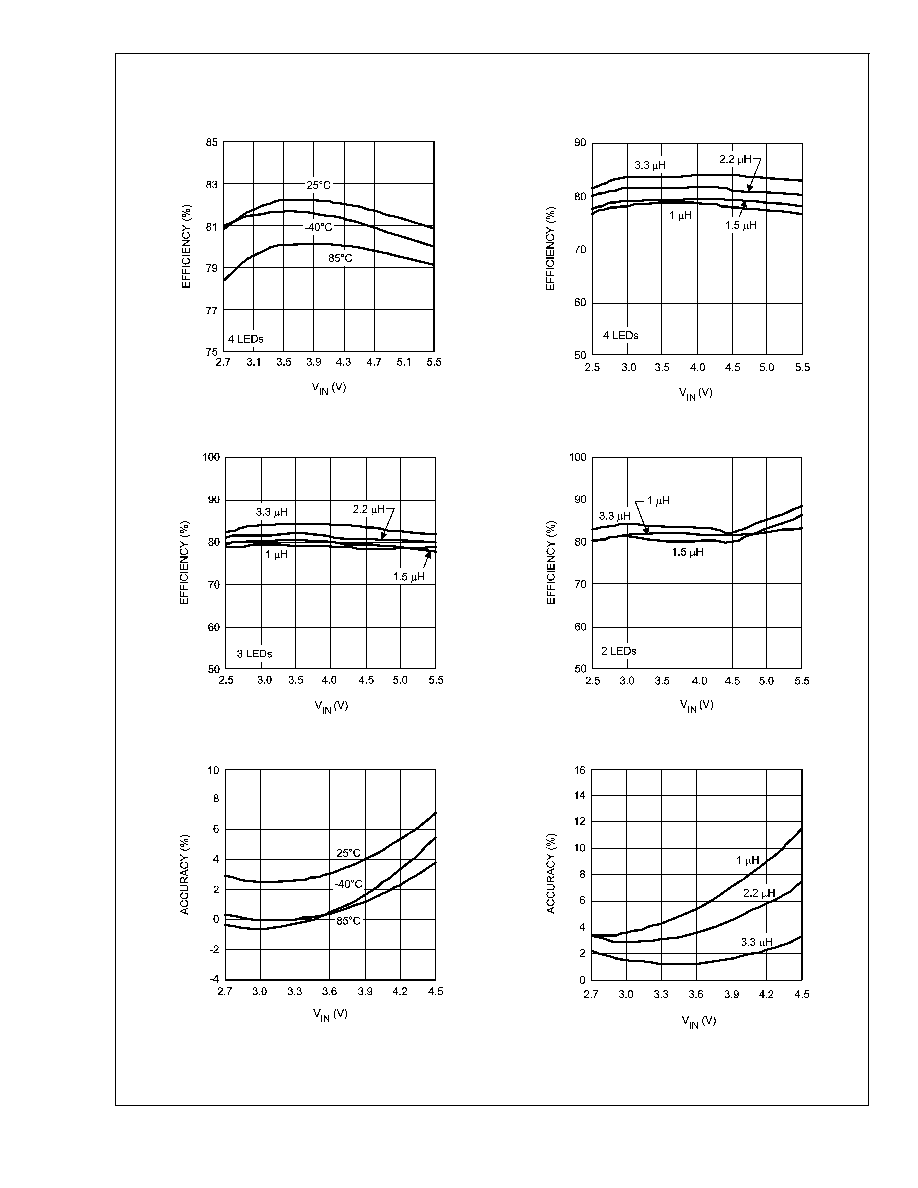
Typical Performance Characteristics
(See Typical Application Circuit : V
IN
= 3.6V, C
IN
= 4.7µF and
C
OUT
= 1µF, L = 2.2µH and 4 LEDs. T
A
= +25∞C, unless otherwise stated.)
Efficiency vs V
IN
Efficiency vs V
IN
20160251
20160231
Efficiency vs V
IN
Efficiency vs V
IN
20160232
20160233
I
OUT_ACCURACY
vs V
IN
I
OUT_ACCURACY
vs V
IN
20160249
20160250
LM3519
www.national.com
6

Typical Performance Characteristics
(See Typical Application Circuit : V
IN
= 3.6V, C
IN
= 4.7µF and
C
OUT
= 1µF, L = 2.2µH and 4 LEDs. T
A
= +25∞C, unless otherwise stated.) (Continued)
I
OUT
vs V
IN
I
OUT
vs V
IN
20160234
20160235
I
OUT
vs V
IN
I
OUT
vs PWM Duty Cycle
(V
IN
= 3.6V, L = 2.2µH)
20160253
20160260
I
OUT
vs PWM Duty Cycle
(V
IN
= 3.6V, L = 2.2µH)
I
OUT
vs PWM Duty Cycle
(V
IN
= 3.6V, L = 1µH)
20160261
20160259
LM3519
www.national.com
7

Typical Performance Characteristics
(See Typical Application Circuit : V
IN
= 3.6V, C
IN
= 4.7µF and
C
OUT
= 1µF, L = 2.2µH and 4 LEDs. T
A
= +25∞C, unless otherwise stated.) (Continued)
I
OUT
vs PWM Duty Cycle
(V
IN
= 3.6V, L = 1µH)
Switching Frequency vs V
IN
20160244
20160207
Switching Frequency vs V
IN
Switching Frequency vs V
IN
20160209
20160245
Switching Frequency vs V
IN
Peak Inductor Current vs V
IN
20160246
20160204
LM3519
www.national.com
8

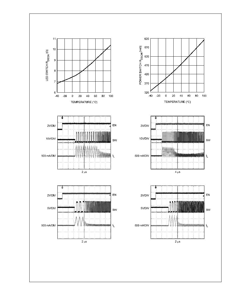
Typical Performance Characteristics
(See Typical Application Circuit : V
IN
= 3.6V, C
IN
= 4.7µF and
C
OUT
= 1µF, L = 2.2µH and 4 LEDs. T
A
= +25∞C, unless otherwise stated.) (Continued)
Peak Inductor Current vs V
IN
Peak Inductor Current vs V
IN
20160206
20160208
Current Limit vs V
IN
(4LEDs, 1µH)
Current Limit vs V
IN
20160247
20160248
Iq (non switching) vs Temperature
Iq (switching) vs Temperature
20160255
20160256
LM3519
www.national.com
9
Typical Performance Characteristics
(See Typical Application Circuit : V
IN
= 3.6V, C
IN
= 4.7µF and
C
OUT
= 1µF, L = 2.2µH and 4 LEDs. T
A
= +25∞C, unless otherwise stated.) (Continued)
LED Switch R
DS_ON
vs Temperature
Power Switch R
DS_ON
vs Temperature
20160257
20160258
Start-up, (V
IN
= 3.6V, 4LEDs, 2.2µH)
Start-up (V
IN
= 3.6V, 4LEDs, 3.3µH)
20160210
20160219
Start-up (V
IN
= 3.6V, 2LEDs, 3.3µH)
Start-up, (V
IN
= 3.6V, 2LEDs, 2.2µH)
20160220
20160211
LM3519
www.national.com
10

Typical Performance Characteristics
(See Typical Application Circuit : V
IN
= 3.6V, C
IN
= 4.7µF and
C
OUT
= 1µF, L = 2.2µH and 4 LEDs. T
A
= +25∞C, unless otherwise stated.) (Continued)
Typical Switching Waveform
(V
IN
= 3.6V, 4LEDs, 3.3µH)
Typical Switching Waveform
(V
IN
= 3.6V, 4LEDs, 2.2µH)
20160218
20160212
Typical Switching Waveform
(V
IN
= 3.6V, 3LEDs, 2.2µH)
Typical Switching Waveform
(V
IN
= 3.6V, 2LEDs, 2.2µH)
20160214
20160215
Typical Switching Waveform
(V
IN
= 3.6V, 3LEDs, 1µH)
Typical Switching Waveform
(V
IN
= 3.6V, 4LEDs, 1µH)
20160228
20160229
LM3519
www.national.com
11

Application Information
CAPACITOR SELECTION
To minimize output and input voltage ripple, low equivalent
series resistance (ESR) ceramic capacitors are the best
choice to use for the input and output filters. For most display
applications, a 4.7µF capacitor is recommended for C
IN
and
1µF for C
OUT
.
Larger output capacitors can be used to reduce ripple volt-
age. To guarantee good performance, a minimum of 0.47µF
C
OUT
is required to trade off for large ripple voltage. Care
must be taken to account for the true capacitance of a
multilayer ceramic capacitor. Smaller case size capacitors
typically have less capacitance for a given bias voltage as
compared to a larger case size capacitor with the same bias
voltage. Please confirm with capacitor manufacturer data
before selecting the capacitor.
Some recommended capacitor manufacturers include but
are not limited to:
Manufacturer
Description
Case Size
AVX
06033D105MAT-25V
0603
06036D475MAT-6.3V
0603
TDK
C2012X5R1A475M-10V
0805
Taiyo Yuden
TMK212BJ105KG-J
0805
EM212BJ475MG-16V
0805
muRata
GRM40-034B105K25
0805
GRM39X5R475K6.3
0603
INDUCTOR SELECTION
In order to maintain sufficient inductance, the saturation
current rating of the inductor used with the LM3519 should
be higher than the peak inductor current in the target appli-
cation. Inductors with low DCR values have less power loss
and higher efficiency. Larger inductor values such as 2.2µH
and 3.3µH can be used to optimize efficiency, frequency and
peak current. If 1µH is used, the peak inductor current,
frequency will be higher and the efficiency will be lower. Note
that the switching frequency ranges will be higher at lower
inductance. Typical frequency range is between 4 to 8MHz
for 1µH, 2 to 5MHz for 2.2µH and 2 to 4MHz for 3.3µH over
the input range. Below is a sample list of low profile induc-
tors.
Some recommended inductor manufacturers include but
are not limited to:
Manufacturer
L
Case Size
I
SAT
CoilCraft:
DO3314-102
1µH
3.3x3.3x1.4mm
2.1A
DO3314-222
2.2µH
1.6A
DO3314-332
3.3µH
1.4A
Coilcraft:
LPO3310-102ML
1µH
3.3x3.3x1.0 mm
1.6A
LPO3310-222ML
2.2µH
1.1A
LPO3310-332ML
3.3µH
0.95A
Cooper:
SD31121R0
1µH
3.1x3.1x1.4 mm
2.07A
SD3114-2R2
2.2µH
1.48A
SD3114-3R3
3.3uH
1.15A
Taiyo Yuden:
NR3015T1R0N
1µH
3.0x3.0x1.5 mm
2.1A
NR3015T2R2M
2.2µH
1.48A
NR3015T3R3M
3.3µH
1.21A
DIODE SELECTION
Diodes with low forward voltage ratings (V
F
) and low junction
capacitance magnitudes (C
J
or C
T
or C
D
) are conducive to
high efficiency. The chosen diode must have a reverse
breakdown voltage rating (V
R
and/or V
RRM
) that is larger
than the output voltage. The following criteria should be
followed when choosing a diode:
1.
V
R
(Diode Blocking Voltage Range) and V
RRM
(Diode
Peak Repetitive Reverse Voltage Rating)
>
V
OUT
(Out-
put Voltage)
2.
I
F
or I
O
(Diode Average Forward Current Rating)
I
LOAD
(Load Current)
3.
I
FRM
(Diode Peak Repetitive Forward Current Rating)
I
Lpeak
(Peak Inductor Current)
Some recommended diode manufacturers include but are
not limited to:
Maufacturer
Description
Vishay
SS12(1A/20V)
SS14(1A/40V)
SS16(1A/60V)
Central Semiconductor
CMSH1- 40M(1A/40V)
ONSemi
MBRS1540T3(1.5A/40V)
PWM DIMMING
The LED current is set internally by the LM3519 to 20mA
(typical); dimming control may be realized by applying a
pulse width modulated(PWM) signal to the En pin. For ex-
ample, a 50% duty cycle waveform will produce an average
current of 10mA. A control signal frequency between 17kHz
and 30kHz is suitable for dimming.
Although the LM3519 is capable of operation outside this
frequency range, it is not recommended to operate below
17kHz for the following reasons: 1) frequency below 100Hz
is likely to cause visible flicker in the light emitted by the LED
string. 2) frequency below 17kHz may induce audible noise
due to combinations of some capacitance/PCB. A PWM
frequency above 30kHz is possible but the current linearity
vs duty cycle will be affected.
If it is not possible to operate the dimming control above
17kHz, audible noise emission may be minimized by using
capacitors with low susceptibility to piezoelectric induced
stresses, such as poly film designs. Minimum audible noise
is most likely to occur when the PWM frequency is less than
2kHz. It is recommended that any application using a PWM
control signal below 17kHz be thoroughly evaluated for un-
desirable audible or visible noise.
DRIVING 2 LEDs
The LM3519 is optimized to drive up to 4LEDs. When driving
2LEDs, a minimum inductance of 2.2µH is required to main-
tain good loop regulation and current accuracy. If a smaller
inductor is used, the LED current will have more variation
with input voltage than a typical application. The following
curve illustrates the behavior.
LM3519
www.national.com
12

Application Information
(Continued)
I
OUT
vs V
IN
20160239
LAYOUT GUIDELINES
The input capacitor, C
IN
, must be placed close to the
LM3519. Placing C
IN
close to the device will reduce the
metal trace resistance effect on input voltage ripple. Metal
trace connections for the C
OUT
capacitor can increase the
effective series resistance, which affects output voltage
ripple and efficiency. Trace connections to the inductor
should be short and wide to reduce power dissipation, in-
crease overall efficiency and reduce EMI radiation. The di-
ode, like the inductor, should have trace connections that are
short and wide to reduce power dissipation and increase
overall efficiency. For more details regarding layout guide-
lines for switching regulators, refer to Applications Note AN-
1149.
LM3519
www.national.com
13

Physical Dimensions
inches (millimeters) unless otherwise noted
6-Lead SOT23-6 Package
NS Package Number MK06A
National does not assume any responsibility for use of any circuitry described, no circuit patent licenses are implied and National reserves
the right at any time without notice to change said circuitry and specifications.
For the most current product information visit us at www.national.com.
LIFE SUPPORT POLICY
NATIONAL'S PRODUCTS ARE NOT AUTHORIZED FOR USE AS CRITICAL COMPONENTS IN LIFE SUPPORT DEVICES OR SYSTEMS
WITHOUT THE EXPRESS WRITTEN APPROVAL OF THE PRESIDENT AND GENERAL COUNSEL OF NATIONAL SEMICONDUCTOR
CORPORATION. As used herein:
1. Life support devices or systems are devices or systems
which, (a) are intended for surgical implant into the body, or
(b) support or sustain life, and whose failure to perform when
properly used in accordance with instructions for use
provided in the labeling, can be reasonably expected to result
in a significant injury to the user.
2. A critical component is any component of a life support
device or system whose failure to perform can be reasonably
expected to cause the failure of the life support device or
system, or to affect its safety or effectiveness.
BANNED SUBSTANCE COMPLIANCE
National Semiconductor manufactures products and uses packing materials that meet the provisions of the Customer Products
Stewardship Specification (CSP-9-111C2) and the Banned Substances and Materials of Interest Specification (CSP-9-111S2) and contain
no ``Banned Substances'' as defined in CSP-9-111S2.
Leadfree products are RoHS compliant.
National Semiconductor
Americas Customer
Support Center
Email: new.feedback@nsc.com
Tel: 1-800-272-9959
National Semiconductor
Europe Customer Support Center
Fax: +49 (0) 180-530 85 86
Email: europe.support@nsc.com
Deutsch Tel: +49 (0) 69 9508 6208
English
Tel: +44 (0) 870 24 0 2171
FranÁais Tel: +33 (0) 1 41 91 8790
National Semiconductor
Asia Pacific Customer
Support Center
Email: ap.support@nsc.com
National Semiconductor
Japan Customer Support Center
Fax: 81-3-5639-7507
Email: jpn.feedback@nsc.com
Tel: 81-3-5639-7560
www.national.com
LM3519
High
Frequency
Boost
White
LED
Driver
with
High-Speed
PWM
Brightness
Control