 | –≠–ª–µ–∫—Ç—Ä–æ–Ω–Ω—ã–π –∫–æ–º–ø–æ–Ω–µ–Ω—Ç: LM3520 | –°–∫–∞—á–∞—Ç—å:  PDF PDF  ZIP ZIP |
LM3520
Integrated White LED Driver with Organic LED Display
Power Supply
General Description
The LM3520 is a dual step-up DC/DC converter, designed to
drive up to 5 white LEDs with a constant current and to
power an organic LED display with a constant voltage.
A single external resistor is used to set the maximum LED
current. The LED current can be adjusted by applying a
PWM signal to the EN pin. For higher efficiency the LM3520
operates with pulse frequency modulation (PFM) control
scheme when the sub-display is enabled. When Main dis-
play is enabled, the device is operating in PWM mode.
Overvoltage protection circuitry and a 1MHz switching fre-
quency allow for the use of small, low cost external compo-
nents.
Additional features include a low-side NFET switch that can
turn off the LED string with no DC current path to ground.
The LM3520 is available in a small 14-pin thermally-
enchanced LLP package.
Features
n
Integrated OLED and white-LED driver
n
80% efficiency
n
Drives up 5 LEDs at 20mA/3.6V and 4 LEDs at
30mA/3.6V for main-display
n
Up to 20V
@
50mA/3.6V for sub-display
n
True shutdown isolation
n
Small External Components
n
1 MHz Switching Frequency
n
23V OverVoltage Protection
n
Wide Input Voltage Range: 2.7V to 5.5V
n
Cycle-By-Cycle Current Limit
n
PWM Dimming Control
n
Low Profile 14-Pin LLP(3mm x 4mm x 0.8mm)
Applications
n
Flip-phones/Clam-shell Cellular Phones
n
Handheld Devices
n
High-fashion cellular phones
n
White LED Backlighting
n
Digital Cameras
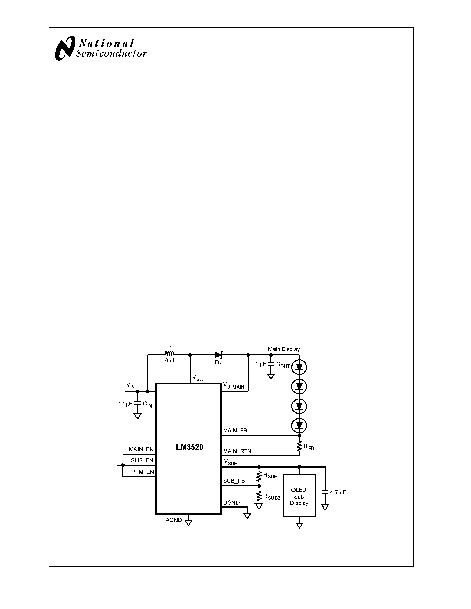
Typical Applications
20128803
Main Display with OLED Sub Display
PRELIMINARY
February 2005
LM3520
Integrated
White
LED
Driver
with
Organic
LED
Display
Power
Supply
© 2005 National Semiconductor Corporation
DS201288
www.national.com
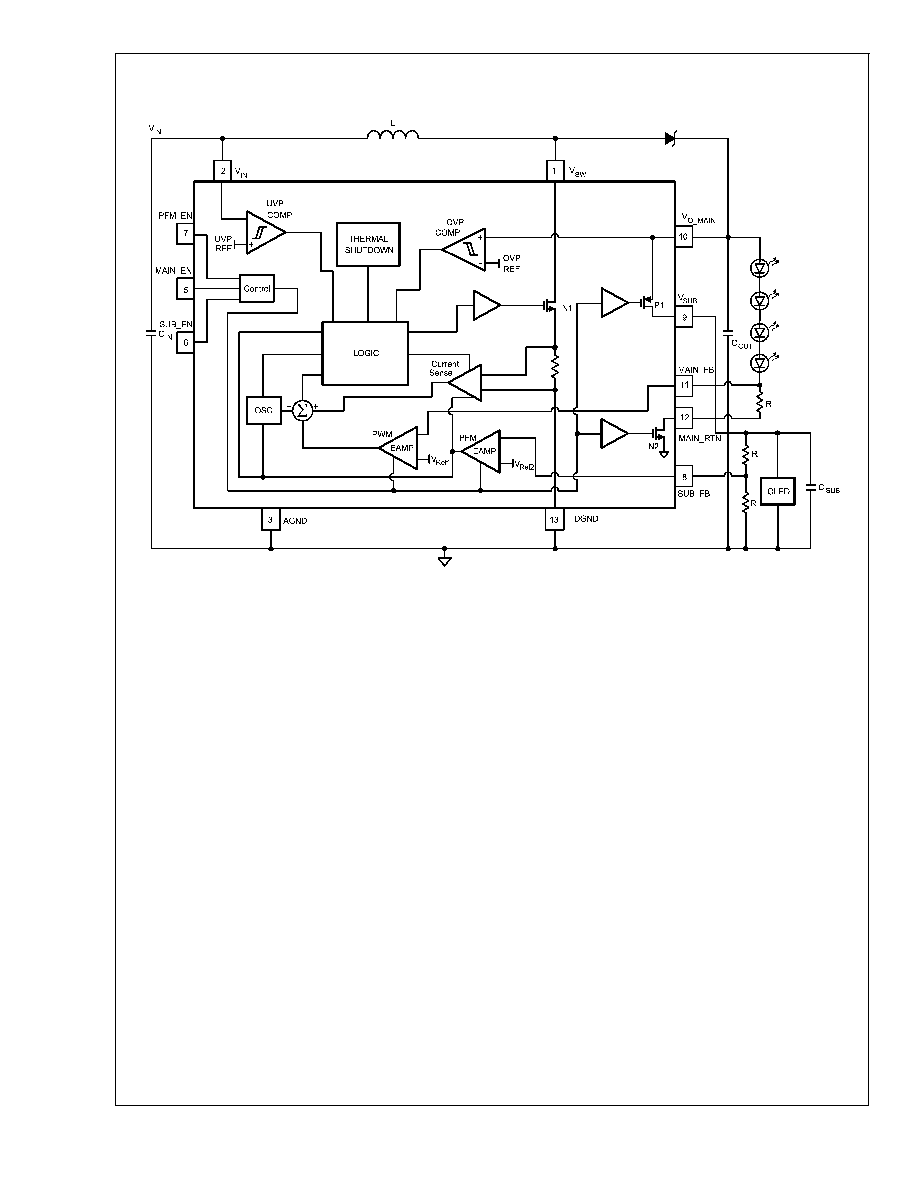
Functional Block Diagram
20128802
FIGURE 1. Functional Block Diagram
LM3520
www.national.com
2

Pin Description
Pin #
Pin Name
Description
1
V
SW
Switching Voltage
2
V
IN
Input Voltage
3
AGND
Analog Ground
4
NC
No Connect
5
MAIN_EN
Main Enable
6
SUB_EN
Sub Display Enable
7
PFM_EN
PFM mode: OLED sub-display, pin must be tied to SUB_EN
8
SUB_FB
Sub Display Feedback
9
V
SUB
Sub Display Power Supply Voltage
10
V
O_MAIN
Main Output Voltage
11
MAIN_FB
Main Display Feedback
12
MAIN_RTN
Main Display Return Voltage
13
DGND
Digital Ground
14
NC
No Connect
Ordering Information
Order Number
Package
NSC Package
Marking
Supplied As
LM3520SD
LLP-14
L133B
1000 units, Tape and Reel
LM3520SDX
L133B
4500 units, Tape and Reel
LM3520
www.national.com
3
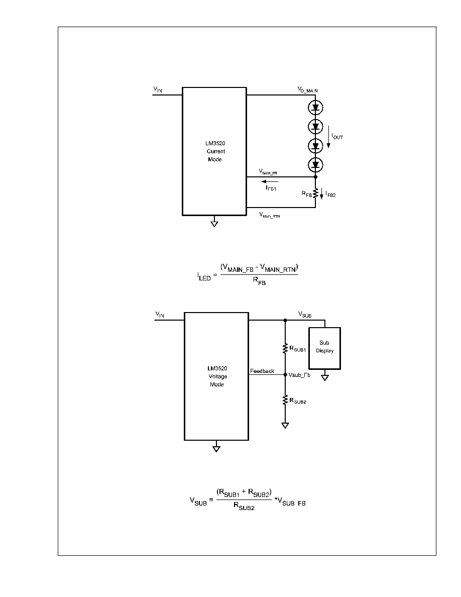
Operation Modes
LM3520 has two operating modes; Figure 2 shows main
display in PWM current mode operation, the appropriate
selection of R
FB
resistor in series with four white LEDs set
the output current driving the main display. Figure 3 shows
Sub display in PFM mode, the appropriate selection of
R
SUB1
and R
SUB2
resistors set the output voltage driving the
OLED subdisplay.
20128806
20128807
* Note: The current I
FB1
is very small and is negligible.
20128804
FIGURE 2. Main Display
20128805
FIGURE 3. Sub Display
LM3520
www.national.com
4
Absolute Maximum Ratings
(Note 1)
If Military/Aerospace specified devices are required,
please contact the National Semiconductor Sales Office/
Distributors for availability and specifications.
V
IN
-0.3V to +7.5V
V
O_MAIN
-0.3V to +25V
V
SW
-0.3V to V
OUT
+0.3V
Main_FB, Main_RTN
-0.3V to +7.5V
MAIN_EN, PFM_EN &
SUB_EN(Note 2)
-0.3V to +7.5V
Continuous Power Dissipation
(Note 3)
Internally Limited
Maximum Junction Temperature
(T
J-MAX
)
+150∞C
Storage Temperature Range
-65∞C to +150∞C
Maximum Lead Temperature
(Soldering, 10 sec)
+265∞C
ESD Rating (Note 4)
Human Body Model:
Machine Model:
2.0 kV
200V
Operating Ratings
Input Voltage Range
2.7V to 5.5V
Junction Temperature (T
J
) Range
-40∞C to +125∞C
Ambient Temperature (T
A
) Range
(Note 3)
-40∞C to +85∞C
Thermal Properties
Junction-to-Ambient Thermal Resistance (
JA)
,
55∞C/W
Leadless Lead frame Package (Note 5)
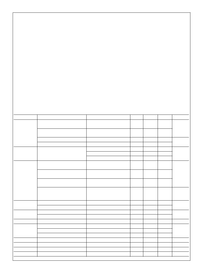
Electrical Characteristics
(Notes 6, 7) Limits in standard typeface are for T
J
= +25∞C. Limits in boldface
type apply over the full operating junction temperature range (-40∞C
= T
J
+125∞C). Unless otherwise noted: specifications
apply to the LM3520. V
IN
= 3.6V, V(En)
>
1.0V, C
IN
= 10 µF (Note 8).
Symbol
Parameter
Conditions
Min
Typ
Max
Units
Enable
Threshold
MAIN_EN = low
SUB_EN = low
0.3
V
MAIN_EN = high
SUB_EN = high
0.95
PFM_EN = low
0.3
V
PFM_EN = high
0.95
I
EN
Enable Pin Current
MAIN_EN = 3.6V (Note 10)
3
5
µA
SUB_EN = 3.6V (Note 10)
3
5
PFM_EN = 3.6V
3
5
I
Q
Quiescent Current, Device Not
Switching (PWM mode)
MAIN_FB
>
0.5V
0.5
1.3
mA
Quiescent Current, Device Not
Switching (PFM mode)
SUB_FB
>
1.0V
0.25
0.45
Quiescent Current, Device
Switching
MAIN_FB = 0V or SUB_FB =
0V (open loop)
1.75
4.5
Power Off Current (Shutdown)
MAIN_EN = low
SUB_EN = low
PFM_EN = low
0.1
2
µA
V
FB
Feedback Voltage (MAIN_FB)
V
IN
= 3.6V
0.455
0.5
0.545
V
Feedback Voltage (SUB_FB)
V
IN
= 3.6V
1.18
1.23
1.28
I
B
FB Pin Leakage Current
MAIN_FB = 0.5V (Note 9)
10
nA
FB Pin Bias Current
SUB_FB = 1.0V (Note 9)
50
I
Current Limit
Switch Current Limit
V
MAIN_FB
= 0V, V
IN
= 3.6V
0.518
0.7
0.917
A
R
DS
(ON)
Main_Switch R
DS
(ON), N1
I
SW
= 300 mA
0.5
PMOS Switch R
DS
(ON), P1
I
PMOS
= 20 mA
3
MAIN_RTN R
DS
(ON), N2
I
Main_RTN
= 30 mA
3
I
main_RTN_leakage
Main_RTN Leakage Current
V
Main_RTN
= 0.5V, V
IN
= 3.6V
0.2
µA
D
Limit
Duty Cycle Limit at PWM & PFM
V
FB
= 0V, V
IN
= 3.6V
90
%
F
SW
Switching Frequency
V
IN
= 3.6V
0.8
1.1
1.4
MHz
I
Leak
Switch Leakage Current
V
SW
= 24V
0.01
0.5
µA
LM3520
www.national.com
5