LM2524D/LM3524D
Regulating Pulse Width Modulator
General Description
The LM3524D family is an improved version of the industry
standard LM3524. It has improved specifications and addi-
tional features yet is pin for pin compatible with existing 3524
families. New features reduce the need for additional exter-
nal circuitry often required in the original version.
The LM3524D has a
±
1% precision 5V reference. The cur-
rent carrying capability of the output drive transistors has
been raised to 200 mA while reducing V
CEsat
and increasing
V
CE
breakdown to 60V. The common mode voltage range of
the error-amp has been raised to 5.5V to eliminate the need
for a resistive divider from the 5V reference.
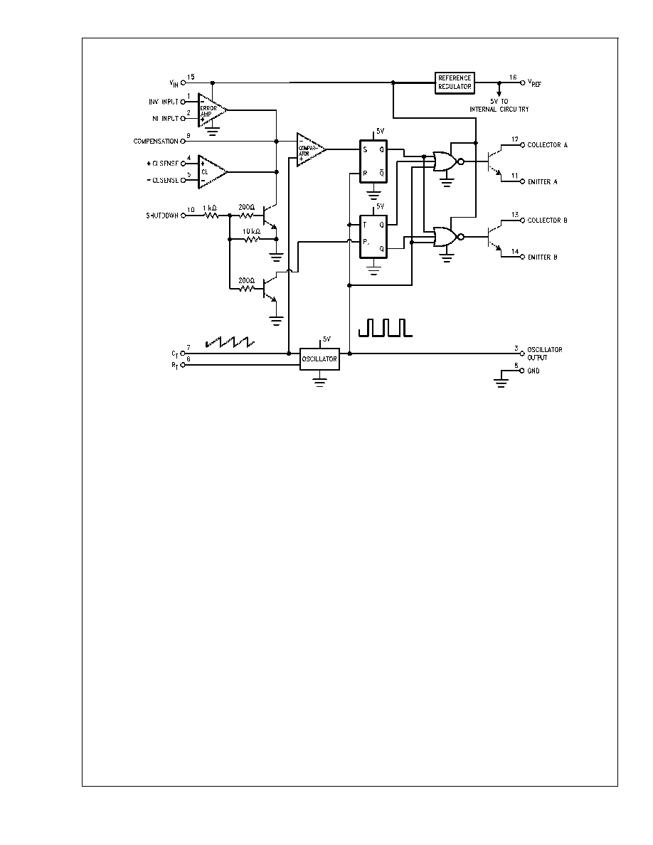
In the LM3524D the circuit bias line has been isolated from
the shut-down pin. This prevents the oscillator pulse ampli-
tude and frequency from being disturbed by shut-down. Also
at high frequencies (
.300 kHz) the max. duty cycle per
output has been improved to 44% compared to 35% max.
duty cycle in other 3524s.
In addition, the LM3524D can now be synchronized exter-
nally, through pin 3. Also a latch has been added to insure
one pulse per period even in noisy environments. The
LM3524D includes double pulse suppression logic that in-
sures when a shut-down condition is removed the state of
the T-flip-flop will change only after the first clock pulse has
arrived. This feature prevents the same output from being
pulsed twice in a row, thus reducing the possibility of core
saturation in push-pull designs.
Features
n
Fully interchangeable with standard LM3524 family
n
±
1% precision 5V reference with thermal shut-down
n
Output current to 200 mA DC
n
60V output capability
n
Wide common mode input range for error-amp
n
One pulse per period (noise suppression)
n
Improved max. duty cycle at high frequencies
n
Double pulse suppression
n
Synchronize through pin 3
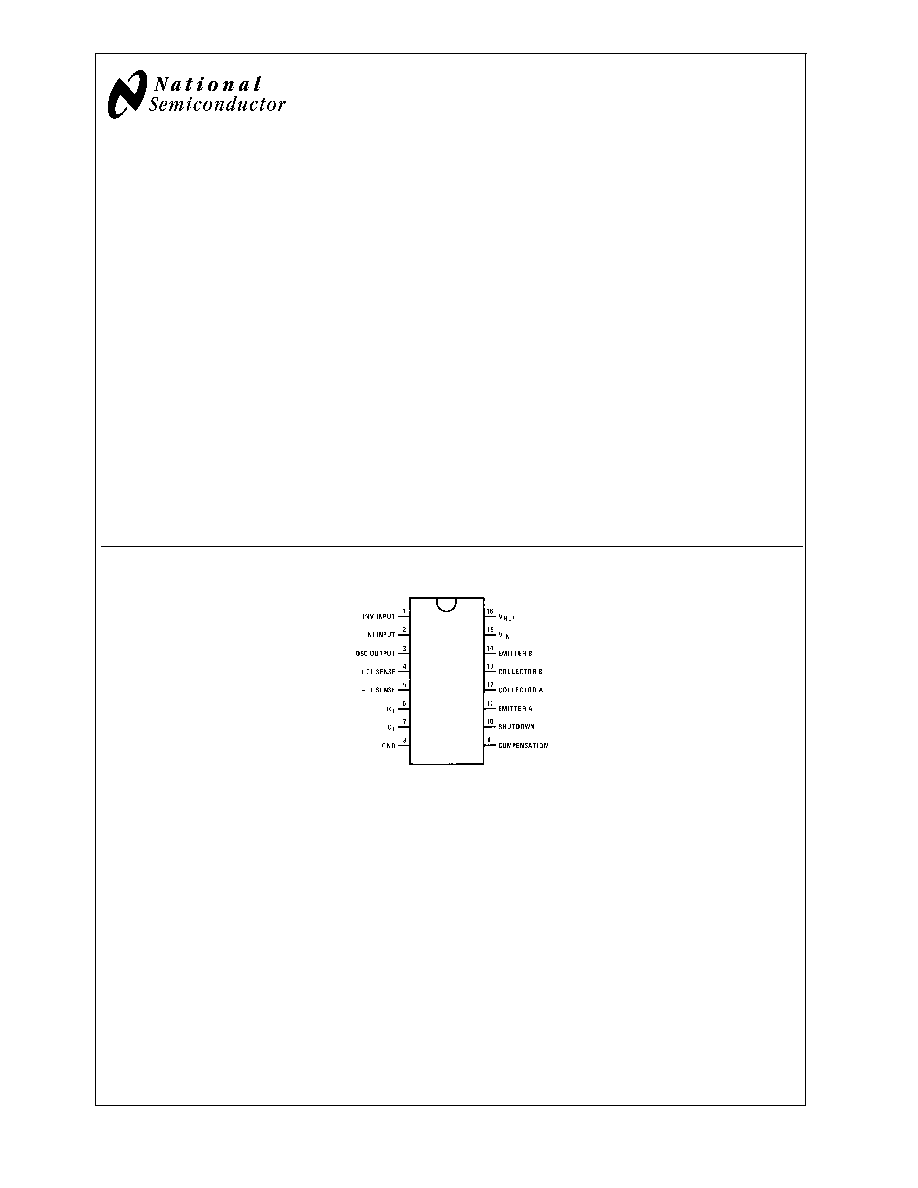
Connection Diagram
00865002
Top View
Order Number LM2524DN or LM3524DN
See NS Package Number N16E
Order Number LM3524DM
See NS Package Number M16A
March 2005
LM2524D/LM3524D
Regulating
Pulse
W
idth
Modulator
© 2005 National Semiconductor Corporation
DS008650
www.national.com

Absolute Maximum Ratings
(Note 5)
If Military/Aerospace specified devices are required,
please contact the National Semiconductor Sales Office/
Distributors for availability and specifications.
Supply Voltage
40V
Collector Supply Voltage
(LM2524D)
55V
(LM3524D)
40V
Output Current DC (each)
200 mA
Oscillator Charging Current (Pin 7)
5 mA
Internal Power Dissipation
1W
Operating Junction Temperature
Range (Note 2)
LM2524D
-40∞C to +125∞C
LM3524D
0∞C to +125∞C
Maximum Junction Temperature
150∞
Storage Temperature Range
-65∞C to +150∞C
Lead Temperature (Soldering 4 sec.)
M, N Pkg.
260∞C
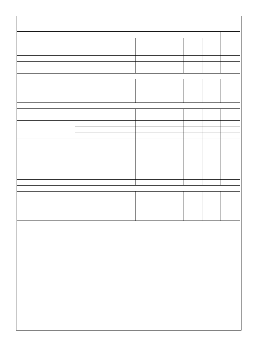
Electrical Characteristics
(Note 1)
LM2524D
LM3524D
Symbol
Parameter
Conditions
Tested
Design
Tested
Design
Units
Typ
Limit
Limit
Typ
Limit
Limit
(Note 3)
(Note 4)
(Note 3)
(Note 4)
REFERENCE SECTION
V
REF
Output Voltage
5
4.85
4.80
5
4.75
V
Min
5.15
5.20
5.25
V
Max
V
RLine
Line Regulation
V
IN
= 8V to 40V
10
15
30
10
25
50
mV
Max
V
RLoad
Load Regulation
I
L
= 0 mA to 20 mA
10
15
25
10
25
50
mV
Max
Ripple Rejection
f = 120 Hz
66
66
dB
I
OS
Short Circuit
V
REF
= 0
25
25
mA Min
Current
50
50
180
200
mA Max
N
O
Output Noise
10 Hz
f 10 kHz
40
100
40
100
µV
rms Max
Long Term
T
A
= 125∞C
20
20
mV/kHr
Stability
OSCILLATOR SECTION
f
OSC
Max. Freq.
R
T
= 1k, C
T
= 0.001 µF
550
500
350
kHz
Min
(Note 7)
f
OSC
Initial
R
T
= 5.6k, C
T
= 0.01 µF
17.5
17.5
kHz
Min
Accuracy
(Note 7)
20
20
22.5
22.5
kHz
Max
R
T
= 2.7k, C
T
= 0.01 µF
34
30
kHz
Min
(Note 7)
38
38
42
46
kHz
Max
f
OSC
Freq. Change
V
IN
= 8 to 40V
0.5
1
0.5
1.0
%
Max
with V
IN
f
OSC
Freq. Change
T
A
= -55∞C to +125∞C
with Temp.
at 20 kHz R
T
= 5.6k,
5
5
%
C
T
= 0.01 µF
V
OSC
Output Amplitude
R
T
= 5.6k, C
T
= 0.01 µF
3
2.4
3
2.4
V
Min
(Pin 3) (Note 8)
t
PW
Output Pulse
R
T
= 5.6k, C
T
= 0.01 µF
0.5
1.5
0.5
1.5
µs
Max
Width (Pin 3)
Sawtooth Peak
R
T
= 5.6k, C
T
= 0.01 µF
3.4
3.6
3.8
3.8
V
Max
Voltage
LM2524D/LM3524D
www.national.com
3
Electrical Characteristics
(Continued)
(Note 1)
LM2524D
LM3524D
Symbol
Parameter
Conditions
Tested
Design
Tested
Design
Units
Typ
Limit
Limit
Typ
Limit
Limit
(Note 3)
(Note 4)
(Note 3)
(Note 4)
TC-V
sense
Sense Voltage T.C.
0.2
0.2
mV/∞C
Common Mode
-0.7
-0.7
V
Min
Voltage Range
V
5
- V
4
= 300 mV
1
1
V
Max
SHUT DOWN SECTION
V
SD
High Input
V
(Pin 2)
- V
(Pin 1)
1
0.5
1
0.5
V
Min
Voltage
150 mV
1.5
1.5
V
Max
I
SD
High Input
I
(pin 10)
1
1
mA
Current
OUTPUT SECTION (EACH OUTPUT)
V
CES
Collector Emitter
I
C
100 µA
55
40
V
Min
Voltage Breakdown
I
CES
Collector Leakage
V
CE
= 60V
Current
V
CE
= 55V
0.1
50
µA
Max
V
CE
= 40V
0.1
50
V
CESAT
Saturation
I
E
= 20 mA
0.2
0.5
0.2
0.7
V
Max
Voltage
I
E
= 200 mA
1.5
2.2
1.5
2.5
V
EO
Emitter Output
I
E
= 50 mA
18
17
18
17
V
Min
Voltage
t
R
Rise Time
V
IN
= 20V,
I
E
= -250 µA
200
200
ns
R
C
= 2k
t
F
Fall Time
R
C
= 2k
100
100
ns
SUPPLY CHARACTERISTICS SECTION
V
IN
Input Voltage
After Turn-on
8
8
V
Min
Range
40
40
V
Max
T
Thermal Shutdown
(Note 2)
160
160
∞C
Temp.
I
IN
Stand By Current
V
IN
= 40V (Note 6)
5
10
5
10
mA
Note 1: Unless otherwise stated, these specifications apply for T
A
= T
J
= 25∞C. Boldface numbers apply over the rated temperature range: LM2524D is -40∞ to 85∞C
and LM3524D is 0∞C to 70∞C. V
IN
= 20V and f
OSC
= 20 kHz.
Note 2: For operation at elevated temperatures, devices in the N package must be derated based on a thermal resistance of 86∞C/W, junction to ambient. Devices
in the M package must be derated at 125∞C/W, junction to ambient.
Note 3: Tested limits are guaranteed and 100% tested in production.
Note 4: Design limits are guaranteed (but not 100% production tested) over the indicated temperature and supply voltage range. These limits are not used to
calculate outgoing quality level.
Note 5: Absolute maximum ratings indicate limits beyond which damage to the device may occur. DC and AC electrical specifications do not apply when operating
the device beyond its rated operating conditions.
Note 6: Pins 1, 4, 7, 8, 11, and 14 are grounded; Pin 2 = 2V. All other inputs and outputs open.
Note 7: The value of a C
t
capacitor can vary with frequency. Careful selection of this capacitor must be made for high frequency operation. Polystyrene was used
in this test. NPO ceramic or polypropylene can also be used.
Note 8: OSC amplitude is measured open circuit. Available current is limited to 1 mA so care must be exercised to limit capacitive loading of fast pulses.
LM2524D/LM3524D
www.national.com
5