 | –≠–ª–µ–∫—Ç—Ä–æ–Ω–Ω—ã–π –∫–æ–º–ø–æ–Ω–µ–Ω—Ç: LM3552 | –°–∫–∞—á–∞—Ç—å:  PDF PDF  ZIP ZIP |

LM3551/LM3552
1A White LED Driver with Flash Timeout Protection
General Description
The LM3551 and LM3552 are fixed frequency, current mode
step-up DC/DC converters with two integrated NFETs that
can be used for precision LED brightness control. The de-
vices are capable of driving loads up to 1A from a single-cell
Li-Ion battery.
The LM3551 and LM3552 can drive one or more high current
flash LEDs either in a high power Flash mode or a lower
power Torch mode using the TORCH/FLASH pin. A program-
mable Timeout function on the FTO pin forces the internal
NFETs to turn off after a certain user defined time. An
external SD pin (LM3551) or EN pin (LM3552) is available to
put the device into low power shutdown mode. During shut-
down, the feedback resistors and the load are disconnected
from the input to avoid leakage current paths to ground.
User programmable soft-start circuitry has been integrated
to eliminate large inrush currents at start-up. Over-voltage
protection circuitry and a 1.25MHz switching frequency allow
for the use of small, low-cost output capacitors with lower
voltage ratings.
The LM3551 and LM3552 are available in a low profile 14 pin
LLP package.
Features
n
Up to 1A total drive current
n
Flash timeout protection
n
Independent Torch/Flash/Shutdown modes
n
LED disconnect in shutdown
n
Programmable soft-start limits inrush current
n
Over-voltage protection
n
Wide voltage range 2.7 to 5.5V
n
1.25MHz constant switching frequency
n
Small, low profile package, non-pullback LLP14 (4mm x
4mm)
Applications
n
White LED Camera Flash
n
White LED Torch (Flashlight)
n
DSC (Digital Still Camera) Flash
n
Cellular Camera Phone Flash
n
PDA Camera Flash
n
Camcorder Torch (Flashlight) lamp
Typical Application Circuits
20151205
August 2005
LM3551/LM3552
1A
White
LED
Driver
with
Flash
T
imeout
Protection
© 2005 National Semiconductor Corporation
DS201512
www.national.com
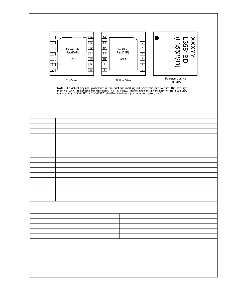
Connection Diagram
14 Pin Dual LLP Package
20151202
NS Package Number SDA14B
Pin Descriptions
Pin
Name
Function
9
V
IN
Input Voltage. Input range: 2.7V to 5.5V.
13
T/F
TORCH/FLASH Pin. Low = Torch Mode, High = Flash Mode
8
SW
Switch Pin
10
OVP
Over Voltage Protection Pin
3
V
C
Compensation network connection. Connected to the output of the voltage error amplifier.
5
SD(LM3551)
EN(LM3552)
Shutdown pin logic input. High = Shutdown, Low = Enabled
Enable pin logic input. High = Enabled, Low = Shutdown
12
FTO
Flash Timeout. External capacitor determines max. duration allowed flash pulse
11
SS
Soft Start Pin
4
FB
Feedback Pin
14
FET-T
Torch FET Drain
2
FET-F
Flash FET Drain
1,7,DAP
GND
Ground
6
AGND
Analog Ground. Connect the ground of the compensation components, C
FTO
and soft start
cap to AGND. AGND must be connected to the GND pin through a low impedance
connection.
Ordering Information
Order Number
SD / EN
Package Marking
Supplied As
LM3551SD
SD
L3551SD
250 units, Tape-and-Reel
LM3551SDX
SD
L3551SD
3000 units, Tape-and-Reel
LM3552SD
EN
L3552SD
250 units, Tape-and-Reel
LM3552SDX
EN
L3552SD
3000 units, Tape-and-Reel
LM3551/LM3552
www.national.com
2

Absolute Maximum Ratings
(Notes 1, 2)
If Military/Aerospace specified devices are required,
please contact the National Semiconductor Sales Office/
Distributors for availability and specifications.
V
IN
pin: Voltage to GND
7.5V
SW pin: Voltage to GND
21V
FB pin: Voltage to GND
7V
V
C
pin: Voltage to GND
1.26V
±
0.3V
SD,T/F pins: Voltage to GND
7.5V
FET-T, FET-F: Voltage to GND
6V
Continuous Power Dissipation (Note 3) Internally Limited
Junction Temperature (T
J-MAX )
150∞C
Storage Temperature Range
-65∞C to +150
Maximum Lead Temperature
(Soldering)
(Note 4)
ESD Rating(Note 5)
Human Body Model
2.0kV
Operating Ratings
(Notes 1, 2)
Input Voltage Range
2.7V to 5.5V
SW Voltage Max. (Note 6)
20V
Junction Temperature (T
J
)
Range
-40∞C to +110∞C
Ambient Temperature (T
A
)
Range (Note 7)
-40∞C to +85∞C
Thermal Properties
Junction-to-Ambient Thermal
Resistance (
JA
), SDA14B
Package (Note 8)
37.3∞C/W
ESD Caution Notice
National Semiconductor recommends that all integrated circuits be handled with appropri-
ate ESD precautions. Failure to observe proper ESD handling techniques can result in damage to the device.
Electrical Characteristics
(Notes 2, 9)
Limits in standard typeface are for T
J
= +25∞ C. Limits in boldface type apply over the full operating junction temperature range
(-40∞C
T
J
+110∞C). Unless otherwise noted, specifications apply to the LM3551 and LM3552 Typical Application Circuit (pg.
1) with: V
IN
= 3.6V, V(SD) = 0V for LM3551 and V(EN) = V
IN
for LM3552, I
LOAD
= 0A (Note 10)
Symbol
Parameter
Conditions
Min
Typ
Max
Units
I
Q
Quiescent Current
FB = V
IN
(Not Switching)
1.47
2.0
mA
I
SD
Shutdown Current
V(SD) = V
IN
LM3551
2.55
5.0
µA
V(EN) = 0V
LM3552
0.1
2.3
I
CL(Note 11)
Switch Current Limit
V
IN
= 3.0V(Note 12)
2.1
A
V
FB
Feedback Voltage
1.2285
1.265
1.2915
V
I
FB(Note 13)
Feedback Pin Bias Current
50
nA
g
m
Error Amp
Transconductance
I = 5µA
135
µmho
A
V
Error Amp Voltage Gain
135
V/V
D
MAX
Maximum Duty Cycle
92.5
%
f
sw
Switching Frequency
0.9
1.25
1.6
MHz
I
SDPIN
Shutdown Pin Current
(LM3551)
V
SD
= 0V
3.0
6
µA
I
ENPIN
Enable Pin Current
(LM3552)
V
EN
= 3.6V
3.0
6
µA
I
T/FPIN
T/F Pin Current
V
T/F
= 0V
26
nA
V
T/F
= V
IN
22
I
L-SW
SW Pin Leakage Current
V
L-SW
= 20V
0.07
8
µA
R
DSON-SW
SW Pin R
DSON
I
SW
= 0.5A
0.165
I
L-T
FET-T Leakage Current
0.1
µA
R
DSON-T
FET-T R
DSON
0.98
I
L-F
FET-F Leakage Current
0.1
µA
R
DSON-F
FET-F R
DSON
0.36
Th
SD/EN
Shutdown/Enable Pin
Threshold
Output High
1.2
V
Output Low
0.3
LM3551/LM3552
www.national.com
3
Electrical Characteristics
(Notes 2, 9) (Continued)
Limits in standard typeface are for T
J
= +25∞ C. Limits in boldface type apply over the full operating junction temperature range
(-40∞C
T
J
+110∞C). Unless otherwise noted, specifications apply to the LM3551 and LM3552 Typical Application Circuit (pg.
1) with: V
IN
= 3.6V, V(SD) = 0V for LM3551 and V(EN) = V
IN
for LM3552, I
LOAD
= 0A (Note 10)
Symbol
Parameter
Conditions
Min
Typ
Max
Units
Th
T/F
T/F Pin Threshold
Output High
1.2
V
Output Low
0.3
UVP
Under Voltage Protection
Thresholds
On Threshold
2.25
2.48
2.70
V
Off Threshold
2.43
2.58
2.77
OVP
Over Voltage Protection
Thresholds
On Threshold
11
12.4
14
V
Off Threshold
9.2
10.6
12
V
FTO
Flash Timeout trip-point
0.99
1.16
1.32
V
I
FTO
Flash Timeout Current
1.12
1.4
1.68
µA
V
SS
Soft-Start Voltage
1.18
1.25
1.32
V
I
SS
Soft-Start Current
10
11.5
13
µA
Note 1: Absolute Maximum Ratings indicate limits beyond which damage to the component may occur. Operating Ratings are conditions under which operation of
the device is guaranteed. Operating Ratings do not imply guaranteed performance limits. For guaranteed performance limits and associated test conditions, see the
Electrical Characteristics tables.
Note 2: All voltages are with respect to the potential at the GND pin.
Note 3: Internal thermal shutdown circuitry protects the device from permanent damage. Thermal shutdown engages at T
J
=140
o
C (typ.) and disengages at
T
J
=120
o
C (typ.).
Note 4: For detailed soldering specifications and information, please refer to National Semiconductor Application Note: AN-1187 for Recommended Soldering
Profiles.
Note 5: The human body model is a 100pF capacitor discharged through a 1.5k
resistor into each pin. (MIL-STD-883 3015.7)
Note 6: Maximum recommended SW pin voltage when the OVP pin is grounded.
Note 7: In applications where high power dissipation and/or poor package thermal resistance is present, the maximum ambient temperature may have to be
derated. Maximum ambient temperature (T
A-MAX
) is dependent on the maximum operating junction temperature (T
J-MAX-OP
= 110
o
C), the maximum power
dissipation of the device in the application (P
D-MAX
), and the junction-to-ambient thermal resistance of the part/package in the application (
JA
), as given by the
following equation: T
A-MAX
= T
J-MAX-OP
≠ (
JA
x P
D-MAX
).
Note 8: Junction-to-ambient thermal resistance is highly application and board-layout dependent. In applications where high maximum power dissipation exists,
special care must be paid to thermal dissipation issues in board design.
Note 9: Min and Max limits are guaranteed by design, test, or statistical analysis. Typical (Typ) numbers are not guaranteed, but do represent the most likely norm.
Unless otherwise specified, conditions for Typ specifications are: V
IN
= 3.6V and T
A
= 25
o
C.
Note 10: C
IN
and C
OUT
,: Low-ESR Surface-Mount Ceramic Capacitors (MLCCs) used in setting electrical characteristics
Note 11: Duty cycle affects current limit due to ramp generator.
Note 12: Current limit at 0% duty cycle. See TYPICAL PERFORMANCE section for Switch Current Limit vs. V
IN
Note 13: Bias current flows into FB pin.
LM3551/LM3552
www.national.com
4

Typical Performance Characteristics
Unless otherwise specified: T
A
= +25∞C; V
IN
= 3.6V; L =
4.7µH, (R
C
= 10k
, C
C
= 4.7nF, C
IN
= C
OUT
= 10µF for Lumiled LED), (R
C
= 27k
, C
C
= 10nF, C
IN
= 10µF, C
OUT
= 4.7µF
for Sharp LED), C
FTO
= 1µF, C
SS
= 0.1µF.
Current Limit vs. Input Voltage
V
OUT
= 5V
Current Limit vs. Input Voltage
V
OUT
= 10V
20151220
Note 14: I
CL
measure when V
OUT
= 95% x V
OUT
(nominal)
20151223
Note 15: I
CL
measure when V
OUT
= 95% x V
OUT
(nominal)
Converter Efficiency vs. Input Voltage
Lumiled Flash LED
Converter Efficiency vs. Input Voltage
Sharp Flash LED
20151211
20151212
LM3551/LM3552
www.national.com
5