LM3570
Low Noise White LED Driver System
General Description
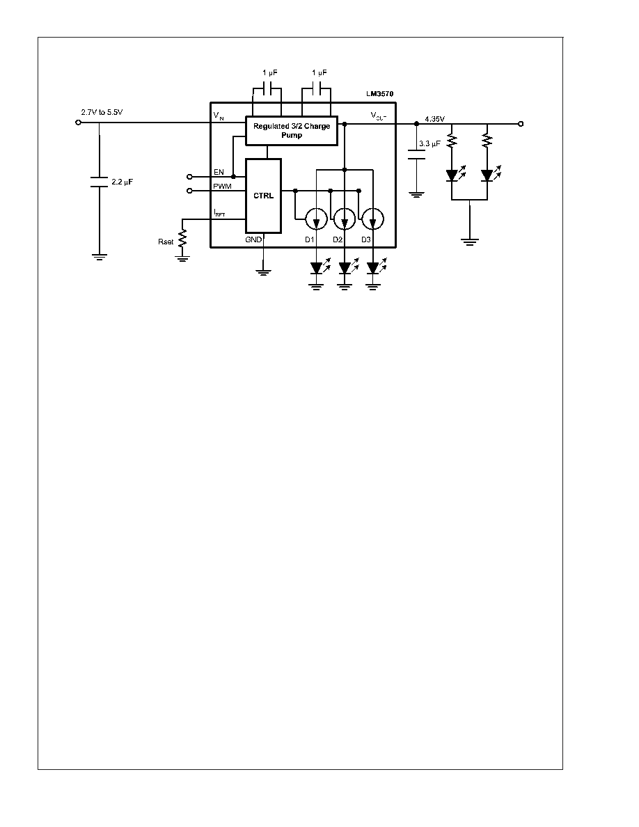
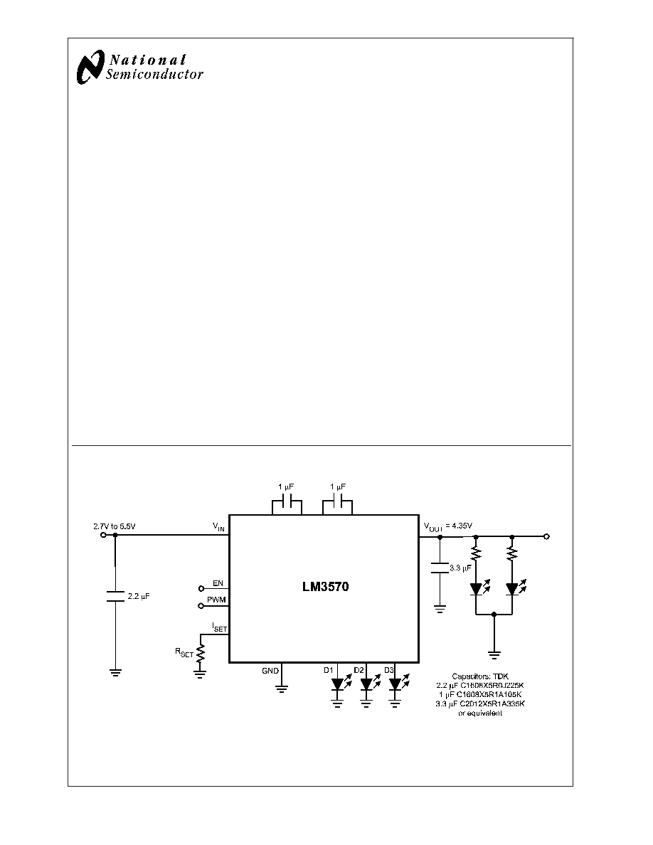
The LM3570 device provides a complete LED driver solution
for wireless handsets and other portable devices using a
display and keypad. With three constant current sources, up
to three white LEDs can be used for display lighting with
excellent current matching (0.3% typ.). The regulated 4.35V
output voltage is perfect for driving auxiliary keypad LEDs in
voltage mode.
The LM3570 utilizes a high efficiency 3/2 CMOS charge-
pump with a pre-regulation loop that minimizes conducted
noise on the input. It accepts an input voltage range from
2.7V to 5.5V and maintains a constant current determined by
the current through an external R
SET
resistor.
The device supplies up to 80mA of total load current to
accommodate any combination of up to three white LEDs,
and additional current from V
OUT
. The switching frequency is
set at 500kHz. (typ.) to keep the conducted noise spectrum
away from sensitive frequencies within portable RF devices.
By applying a pulse width modulated (PWM) signal to the
PWM pin, the user has the ability to independently control
the brightness of the regulated current source outputs with-
out shutting down the regulated output voltage.
Features
n
2.7V to 5.5V Input Voltage
n
Regulated Output Voltage (V
OUT
= 4.35V)
n
Regulated I
Dx
with
±
0.3% matching between constant
current outputs
n
High Efficiency 3/2 Boost function
n
Drives one, two, or three white LEDs with no bias
resistor losses
n
Drives auxiliary keypad LEDS in voltage mode
n
Up to 80mA total output current
n
Active-High Enable
n
Active-High PWM Control Pin for independent control of
current sources
n
Very small solution size
n
1µA(max) shutdown current
n
500kHz switching frequency (typ.)
n
Linear regulation generates predictable noise spectrum
n
LLP-14 package: 4.0mm X 3.0mm X 0.8mm
Applications
n
Portable devices using white or blue LEDs with display
and backlight or frontlight
n
1-Cell LiIon battery-operated equipment including PDAs,
hand-held PCs and cellular phones
Typical Application Circuit
20085021
July 2004
LM3570
Low
Noise
White
LED
Driver
System
© 2004 National Semiconductor Corporation
DS200850
www.national.com
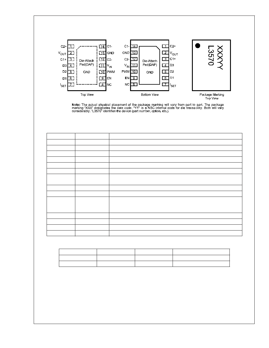
Connection Diagram
LLP-14 DIP Package, 4mmx3mmx0.8mm
NS Package Number SDA14A
20085002
Pin Description
Pin#
Pin Name
Pin Description
1
C2+
Connect this pin to the positive terminal of C2.
2
V
OUT
Regulated Charge pump output (4.35V).
3
C1+
Connect this pin to the positive terminal of C1.
4
D3
Current source output 3. Connect directly to LED.
5
D2
Current source output 2. Connect directly to LED.
6
D1
Current source output 1. Connect directly to LED.
7
I
SET
Current set input. Value of resistor tied between I
SET
and GND sets the Dx
output currents.
8
NC
No Connect
9
EN
Enable Input High = On, Low = Shutdown
10
PWM
Current Source Modulation pin. High = On, Low = Off. Applying a PWM signal
to this pin allows the regulated current sources to be to be modulated without
shutting down the V
OUT
pin and the remainder of the part.
11
V
IN
Power supply voltage input.
12
C2-
Connect this pin to the negative terminal of C2.
13
GND
Ground connection.
14
C1-
Connect this pin to the negative terminal of C1.
Ordering Information
Order Number
Package Type
Package Marking
Supplied As:
LM3570SD
SDA14A
L3570
1000 units on Tape-and-Reel
LM3570SDX
SDA14A
L3570
3500 units on Tape-and-Reel
LM3570
www.national.com
2
Absolute Maximum Ratings
(Notes 1, 2)
If Military/Aerospace specified devices are required,
please contact the National Semiconductor Sales Office/
Distributors for availability and specifications.
VIN pin: Voltage to GND
-0.3V to 6.0V
EN, PWM: Voltage to GND
-0.3V to (V
IN
+
0.3V) w/ 6.0V max
Continuous Power Dissipation
(Note 3)
Internally Limited
Junction Temperature (T
J-MAX
)
150
o
C
Storage Temperature Range
-65
o
C to +150
o
C
Maximum Lead Temperature
(Soldering, 10 sec.)
(Note 4)
ESD Rating(Note 5)
Human Body Model
Machine Model
2.0kV
200V
Operating Ratings
(Notes 1, 2)
Input Voltage Range
2.7V to 5.5V
Junction Temperature (T
J
) Range
-40°C to +105°C
Ambient Temperature (T
A
) Range
(Note 6)
-40°C to +85°C
Thermal Properties
Juntion-to-Ambient Thermal
Resistance (
JA
), LLP14 Package
(Note 7)
45°C/W
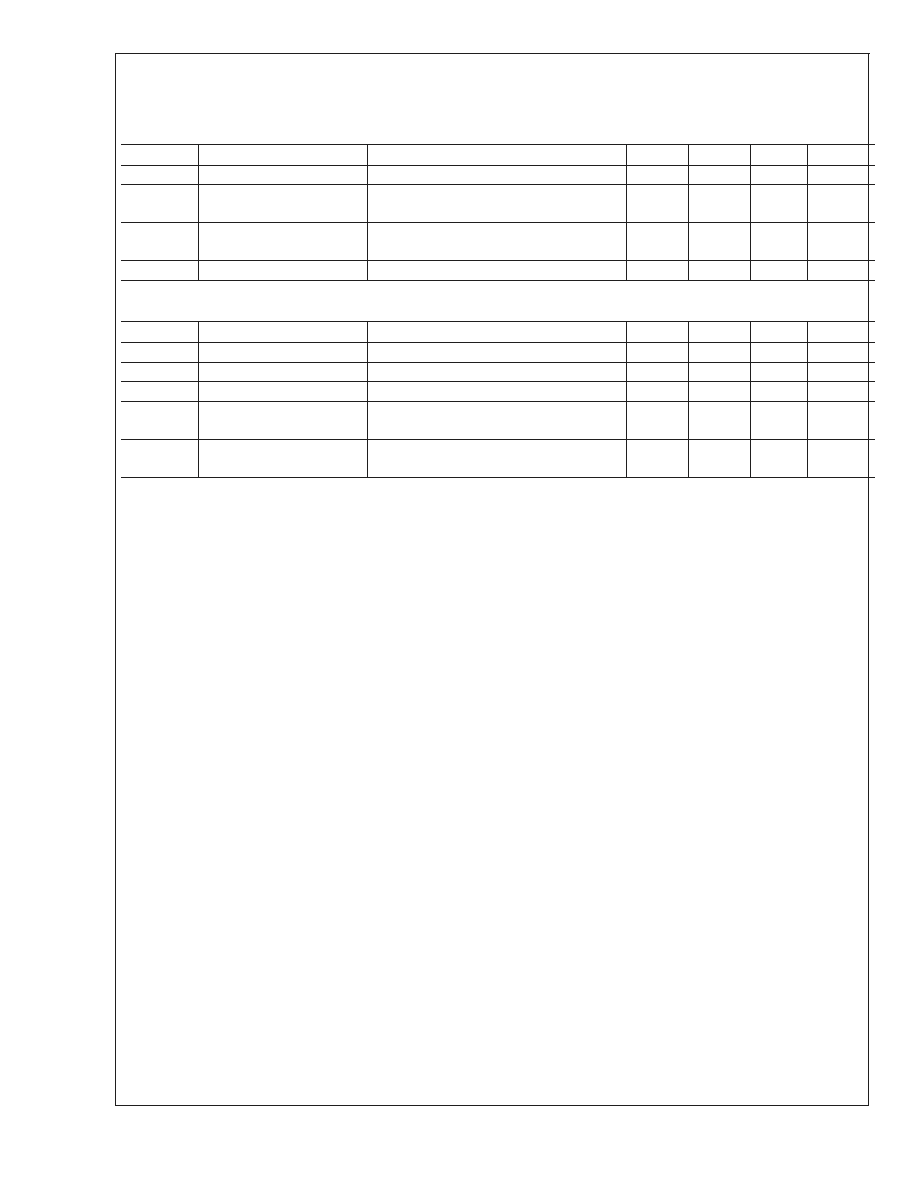
Electrical Characteristics
(Notes 2, 8)
Limits in standard typeface and typical values apply for T
J
= 25
o
C. Limits in boldface type apply over the operating junction
temperature range. Unless otherwise noted, specifications apply to the LM3570 typical Application Circuit (pg.1) with: V
IN
=
3.6V, V
EN
= 3.0V, V
PWM
= 3.0V, V
DX
=3.6V, R
SET
= 6.25k
, C
1
=C
2
=1.0µF, C
IN
=2.2µF, C
OUT
=3.3µF(Note 9)
Symbol
Parameter
Condition
Min
Typ
Max
Units
I
Dx
Output Current Regulation
(All Current Sources Active
Total Current = 3 x I
Dx
)
(Note 10)
3.0V
V
IN
5.5V;
2.5V
V
Dx
3.6V;
R
SET
= 6.25k
;
I
VOUT
= 0mA
18.4
20.0
21.6
mA
3.0V
V
IN
5.5V;
2.5V
V
Dx
3.8V;
R
SET
= 8.35k
;
I
VOUT
= 0mA
13.6
15.0
16.4
3.0V
V
IN
5.5V;
2.5V
V
Dx
3.9V;
R
SET
= 12.5k
;
I
VOUT
= 0mA
10.0
V
OUT
Regulated Output Voltage
3.3V
V
IN
5.5V;
0mA
I
Total
80mA(Note 11)
4.1
4.3
4.6
V
I
Dx-MATCH
Current Matching Between
Any Two Outputs(Note 12)
0.3
%
V
HR
Current Source Headroom
Voltage
(Note 13)
I
Dx
= 95% x I
Dx
(nom.);
R
SET
= 6.25k
;
(I
Dx
(nom.)
20mA)
500
mV
I
Dx
= 95% x I
Dx
(nom.)
R
SET
= 8.35k
;
(I
Dx
(nom.)
15mA)
375
I
Q
Quiescent Supply Current
3.0V
V
IN
5.5V;
R
SET
= open;
No Load Current
1.5
2.0
mA
3.0V
V
IN
5.5V;
R
SET
= 6.25k
;
No Load Current
1.8
I
SD
Shutdown Supply Current
3.0V
V
IN
5.5V;
V(EN) = 0V, V(PWM) = 0V
(Note 14)
0.1
1.0
µA
R
OUT
Charge Pump Output
Resistance
3.0V
V
IN
5.5V
4
LM3570
www.national.com
3
Electrical Characteristics
(Notes 2, 8)
(Continued)
Limits in standard typeface and typical values apply for T
J
= 25
o
C. Limits in boldface type apply over the operating junction
temperature range. Unless otherwise noted, specifications apply to the LM3570 typical Application Circuit (pg.1) with: V
IN
=
3.6V, V
EN
= 3.0V, V
PWM
= 3.0V, V
DX
=3.6V, R
SET
= 6.25k
, C
1
=C
2
=1.0µF, C
IN
=2.2µF, C
OUT
=3.3µF(Note 9)
Symbol
Parameter
Condition
Min
Typ
Max
Units
V
SET
I
SET
Pin Voltage
1.25
V
I
Dx
/ I
SET
Output Current to Current
Set Ratio
100
f
SW
Switching Frequency
(Note 15)
3.0V
V
IN
5.5V
300
500
665
kHz
t
START
Start-up Time
I
Dx
= 90% steady state
250
µs
EN and PWM Pin Characteristics
V
EN-IL
Enable Pin Logic Low
3.0V
V
IN
5.5V
0
0.5
V
V
EN-IH
Enable Pin Logic High
3.0V
V
IN
5.5V
1.0
V
IN
V
V
PWM-IL
PWM Pin Logic Low
3.0V
V
IN
5.5V
0
0.5
V
V
PWM-IH
PWM PinLogic High
3.0V
V
IN
5.5V
1.0
V
IN
V
I
LEAK-EN
Enable Pin Leakage Current
(Note 14)
10
µA
I
LEAK-PWM
PWM Pin Leakage Current
(Note 14)
10
µA
Note 1: Absolute Maximum Ratings indicate limits beyond which damage to the component may occur. Operating Ratings are conditions under which operation of
the device is guaranteed. Operating Ratings do not imply guaranteed performance limits. For guaranteed performance limits and associated test conditions, see the
Electrical Characteristics tables.
Note 2: All voltages are with respect to the potential at the GND pin.
Note 3: Internal thermal shutdown circuitry protects the device from permanent damage. Thermal shutdown engages at T
J
=150
o
C (typ.) and disengages at
T
J
=140
o
C (typ.).
Note 4: For detailed soldering specifications and information, please refer to National Semiconductor Application Note 1187: Leadless Leadframe Package
(LLP).
Note 5: The Human body model is a 100pF capacitor discharged through a 1.5k
resistor into each pin. (MIL-STD-883 3015.7) The machine model is a 200pF
capacitor discharged directly into each pin. (EAIJ)
Note 6: In applications where high power dissipation and/or poor package thermal resistance is present, the maximum ambient temperature may have to be
derated. Maximum ambient temperature (T
A-MAX
) is dependent on the maximum operating junction temperature (T
J-MAX-OP
= 125
o
C), the maximum power
dissipation of the device in the application (P
D-MAX
), and the junction-to ambient thermal resistance of the part/package in the application (
JA
), as given by the
following equation: T
A-MAX
= T
J-MAX-OP
(
JA
x P
D-MAX
).
Note 7: Junction-to-ambient thermal resistance is highly application and board-layout dependent. In applications where high maximum power dissipation exists,
special care must be paid to thermal dissipation issues in board design. For more information on these topics, please refer to Application Note 1187: Leadless
Leadframe Package (LLP) and the PCB Layout Considerations and Power Dissipation section of this datasheet.
Note 8: Min and Max limits are guaranteed by design, test, or statistical analysis. Typical (Typ) numbers are not guaranteed, but do represent the most likely norm.
Unless otherwise specified, conditions for Typ specifications are: V
IN
= 3.6V and T
A
= 25
o
C.
Note 9: C
IN
, C
OUT
, C1, and C2 : Low-ESR Surface-Mount Ceramic Capacitors (MLCCs) used in setting electrical characteristics
Note 10: Maximum I
Dx
=20mA
Note 11: I
TOT
is equal to the sum of all I
Dx
currents and the current drawn from V
OUT
. Current can be drawn from any combination of V
OUT
and I
D1
, I
D2
, and I
D3
as long as the maximum current does not exceed 80mA.
Note 12: For the group of the three outputs on a part the following are determined: the maximum output current in the group (MAX), the minimum output current
in the group (MIN), and the average output current of the group (AVG).Two matching numbers are calculated: (MAX-AVG)/AVG and (AVG-MIN)/AVG. The largest
number of the two (worst case) is considered the matching figure for the group. The matching figure for a given part is considered to be the highest matching figure.
The typical specification provided is the most likely norm of the matching figure for all parts.
Note 13: Headroom Voltage is defined as the amount of voltage required across the regulated current sources in order to guarantee the full amount of output current
is realized. V
OUT
V
Dx
= V
HR
. The minimum headroom required is defined as follows: V
HR
(min)
k
HR
x I
Dx
where k
HR
is the headroom proportionality constant
and I
Dx
is the desired controlled diode current. The LM3570 has a k
HR
= 25mV/mA. For more information, please refer to the output current section of this datasheet.
Note 14: The EN and PWM pins have 300k
internal pull-down resistors. When the part is in shutdown, the PWM pin must be tied low to ensure lowest possible
shutdown current.
Note 15: The output switches operate at one eighth of the oscillator frequency, f
OSC
=8xf
SW
LM3570
www.national.com
4