 | ÐлекÑÑоннÑй компоненÑ: LM3595LD | СкаÑаÑÑ:  PDF PDF  ZIP ZIP |
Äîêóìåíòàöèÿ è îïèñàíèÿ www.docs.chipfind.ru
LM3595
Parallel White-LED Driver
General Description
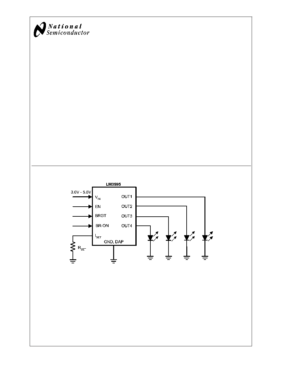
The LM3595 is a parallel white-LED driver that is capable of
driving four white LEDs. It can supply a total output current of
100mA over an input voltage range of 3.0V to 5.5V. The
amount of constant current sourced to the outputs is user
selectable using one external sense resistor.
LM3595 typically draws 0.03µA when placed in shutdown,
and 200µA when operating in the no-load condition. If any of
the outputs are not used, leave the pin(s) unconnected.
Brightness can be controlled by both analog and PWM tech-
niques. A voltage between 0V and 3V may be applied to the
BRGT pin to vary the current. Output current will linearly
track the voltage applied to the BRGT pin. An active-low
level must be present on the BR-ON pin for analog bright-
ness control to be disabled. Alternatively, a PWM signal can
be applied to the EN pin to vary the perceived brightness of
the LED.
The LM3595 uses an active-high enable level. The LM3595
is available in National's LLP-10 package.
Features
n
Regulated I
OUT
with
±
0.5% matching between constant
current outputs
n
Drives one, two, three or four white LED's with no bias
resistors
n
3.0V to 5.5V Input voltage
n
Up to 100mA output current
n
Active-High Enable Pin
n
Analog Brightness Control
n
Very small solution size
n
LLP-10 package: 3.0mm x 3.0mm x 0.8mm
n
Very Low Shutdown current (0.03µA typ.)
Applications
n
Portable devices using white or blue LEDs with display
and backlight or frontlight
n
Keypad LEDs
n
Strobe LEDs
Typical Application Circuit
20072201
August 2003
LM3595
Parallel
White-LED
Driver
© 2003 National Semiconductor Corporation
DS200722
www.national.com
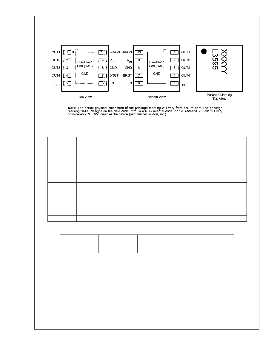
Connection Diagram
LM3595
10-Pin Leadless Leadframe Package (LLP) - 3mm X 3mm
NS Package Number LDA10A
20072202
Pin Description
Pin
Name
Description
9
V
IN
Input Voltage
1,2,3,4
OUT1-4
Current Source Outputs 1- 4 - Connect directly to LED's
5
I
SET
Current Set Input- The resistor value tied between this pin and ground sets the
output current.
6
EN
Active-High Enable Input - A 1M
resistor is connected internally between this
pin and GND to pull the voltage on this pin to 0V, and shut down the part,
when the pin is left floating.
10
BR-ON
Active-High Analog Brightness Control Enable - A voltage of .65 x V
IN
must be
applied to this pin to enable analog brightness control.
7
BRGT
Analog-voltage-controlled Brightness Input - When the BR-ON pin is set high,
the voltage on this pin allows analog control of the LED's brightness. The
recommended voltage range on this pin is 0 - 3 V where 3V is V
BR(MAX)
. The
input impedance of this pin is 300k
.
8, DAP
GND
Ground
Ordering Information
Order Number
Package Number
Package Marking
Supplied as:
LM3595LD
LDA10A
L3595
1000 units on Tape-and-Reel
LM3595LDX
LDA10A
L3595
3500 units on Tape-and-Reel
LM3595
www.national.com
2
Absolute Maximum Ratings
(Notes 1,
2)
If Military/Aerospace specified devices are required,
please contact the National Semiconductor Sales Office/
Distributors for availability and specifications.
V
IN
-0.3V to 6.0V
EN, BR-ON, BRGT
-0.3V to
(V
IN
+ 0.3V) w/
6.0V max
Junction Temperature (T
J-MAX-ABS
)
150°C
Continuous Power Dissiation
(Note 3)
Internally Limited
Storage Temperature Range
-65°C to 150°C
Lead Temperature
(Soldering, 5 Sec.)
260°C
ESD Rating (Note 4)
Human-body model
Machine model
2 kV
200V
Operating Ratings
(Notes 1, 2)
Input Voltage Range (Note 5)
3.0V to 5.5V
Output Voltage Range (Note 5)
2.0V to 5.5V
Junction Temperature Range
(Note 6)
-40°C to 105°C
Ambient Temperature Range
(Note 6)
-40°C to 85°C
Thermal Information
Junction-to-Ambient Thermal
Resistance, LLP-10 Package (
JA
)
(Note 7)
55°C/W
Electrical Characteristics
(Notes 2, 8)
Limits in standard typeface and typical values apply for T
J
= 25
o
C. Limits in boldface type apply over the operating junction
temperature range. Unless otherwise specified: V
IN
= 5V, V
OUTX
= 3.6V, R
SET
= 8.25k
, V(EN) = V
IN
, V(BR-ON) = 0V
Symbol
Parameter
Conditions
Min
Typ
Max
Units
I
OUTX
Output Current Regulation
(Note 5)
3.0V
V
IN
5.5V
2.0V
V
OUTX
(V
IN
- 0.7V)
R
SET
= 4.99k
22.54
(-8%)
24.5
26.46
(+8%)
mA
( % )
3.0V
V
IN
5.5V
2.0V
V
OUTX
(V
IN
- 0.42V)
R
SET
= 8.25k
13.80
(-8%)
15.0
16.20
(+8%)
3.0V
V
IN
5.5V
2.0V
V
OUTX
(V
IN
- 0.28V)
R
SET
= 12.4k
9.20
(-8%)
10.0
10.80
(+8%)
I
OUTX-BRGT
Analog Brightness Control
Current Regulation
V(BRGT) = 3.0V, V(BR-ON) = V
IN
13.83
(-6.5%)
14.8
15.77
(+6.5%)
mA
( % )
V(BRGT) = 0V, V(BR-ON) = V
IN
100
250
µA
I
OUT-MATCH
Current Matching Between
Any Two Outputs
0.5
4
%
V
SET
I
SET
Pin Voltage
1.147
(-6%)
1.22
1.293
(+6%)
V
( % )
I
OUTX
/I
SET
Output Current to Current
Set Ratio
95
(-5%)
100
105
(+5%)
V
HR
Current Source Headroom
Voltage (Note 5)
I
OUT
= 95% x I
OUT
(nom)
R
SET
= 4.99k
(I
OUT
(nom) approx. 25mA)
500
690
mV
I
OUT
= 95% x I
OUT
(nom)
R
SET
= 12.4k
(I
OUT
(nom) approx. 10mA)
200
280
I
Q
Quiescent Supply Current
I
OUTX
= 0mA, V(BR-ON) = V
IN
, R
SET
=
Open
200
300
µA
I
OUTX
= 0mA, V(BR-ON) = V
IN
, R
SET
=
8.25k
350
I
SD
Shutdown Supply Current
EN = 0, V(BR-ON) = V
IN
0.03
1
µA
V
EN-IH
EN Input Logic High
3.0V
V
IN
5.5V
1.2
V
IN
V
V
EN-IL
EN Input Logic Low
3.0V
V
IN
5.5V
0
.5
V
V
BRON-IH
BR-ON Input Logic High
3.0V
V
IN
5.5V
.65 x V
IN
V
IN
V
V
BRON-IL
BR-ON Input Logic Low
3.0V
V
IN
5.5V
0
.35 x V
IN
V
LM3595
www.national.com
3
Electrical Characteristics
(Notes 2, 8)
(Continued)
Limits in standard typeface and typical values apply for T
J
= 25
o
C. Limits in boldface type apply over the operating junction
temperature range. Unless otherwise specified: V
IN
= 5V, V
OUTX
= 3.6V, R
SET
= 8.25k
, V(EN) = V
IN
, V(BR-ON) = 0V
Symbol
Parameter
Conditions
Min
Typ
Max
Units
I
EN
EN Pin Current (Note 9)
V(EN) = 1.5V
1.5
µA
V(EN) = 0V
0
I
BR-ON
BR-ON Pin Current
0
V
BR-ON
V
IN
0
µA
Note 1: Absolute Maximum Ratings indicate limits beyond which damage to the component may occur. Operating Ratings are conditions under which operation
of the device is guaranteed. Operating Ratings do not imply guaranteed performance limits. For guaranteed performance limits and associated test conditions, see
the Electrical Characteristics tables.
Note 2: All voltages are with respect to the potential at the GND pin.
Note 3: Thermal shutdown circuitry protects the device from permanent damage.
Note 4: The Human body model is a 100pF capacitor discharged through a 1.5k
resistor into each pin. The machine model is a 200pF capacitor discharged
directly into each pin. MIL-STD-883 3015.7
Note 5: The operation rating for minimum input voltage, V
MIN
, is limited by V
OUTX
and I
OUTX
as dictated by headroom voltage. The equation, V
MIN
(V
OUTX
+V
HR
),
must be satisfied for the desired output current to be realized. For more information, see the section on Output Current Capability found in this datasheet.
Note 6: In applications where high power dissipation and/or poor package thermal resistance is present, the maximum ambient temperature may have to be
derated. Maximum ambient temperature (T
A-MAX
) is dependent on the maximum operating junction temperature (T
J-MAX-OP
= 105°C), the maximum power
dissipation of the device in the application (P
D-MAX
), and the junction-to ambient thermal resistance of the part/package in the application (
JA
), as given by the
following equation: T
A-MAX
= T
J-MAX-OP
- (
JA
x P
D-MAX
).
Note 7: Junction-to-ambient thermal resistance (
JA
) is taken from a thermal modeling result, performed under the conditions and guidelines set forth in the JEDEC
standard JESD51-7. The test board is a 4-layer FR-4 board measuring 102mm x 76mm x 1.6mm with a 2x1 array of thermal vias. The ground plane on the board
is 50mm x 50mm. Thickness of copper layers are 36µm/18µm/18µm/36µm (1.5oz/1oz/1oz/1.5oz). Ambient temperature in simulation is 22°C, still air. Power
dissipation is 1W. The value of
JA
of the LM3595 in LLP-10 could fall in a range as wide as 50°C/W to 150°C/W (if not wider), depending on PWB material, layout,
and environmental conditions. In applications where high maximum power dissipation exists (high V
IN
, high I
OUT
), special care must be paid to thermal dissipation
issues. For more information on these topics, please refer to Application Note 1187: Leadless Leadframe Package (LLP) and the Power Dissipation and PCB Layout
Considerations sections of this datasheet.
Note 8: All room temperature limits are 100% tested or guaranteed through statistical analysis. All limits at temperature extremes are guaranteed by correlation
using standard Statistical Quality Control methods (SQC). All limits are used to calculate Average Outgoing Quality Level (AOQL). Typical numbers are not
guaranteed, but do represent the most likely norm.
Note 9: The EN pin has an internally connected 1M
pull-down resistor
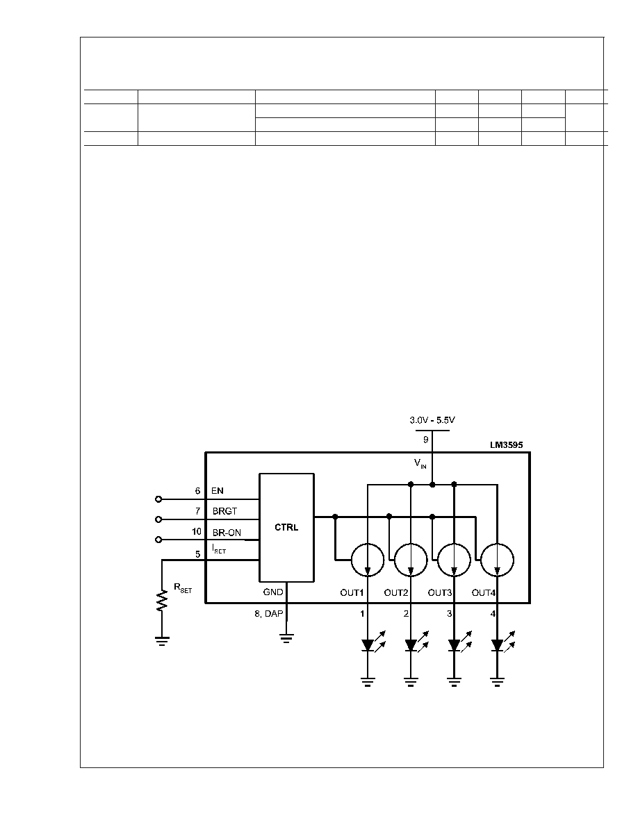
Block Diagram
20072203
LM3595
www.national.com
4
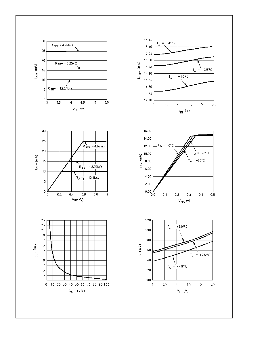
Typical Performance Characteristics
Unless otherwise specified: V
IN
= 5V, BR-ON = 0V, R
SET
=
8.25k
, EN = V
IN
, T
A
= 25°C
Output Current vs. Input Voltage
Output Current vs. Input Voltage
20072207
20072210
Output Current vs. Headroom Voltage
Output Current vs. Headroom Voltage
20072206
20072213
Output Current vs. Current Set Resistor
Quiescent Current vs. Input Voltage (R
SET
= Open)
20072217
20072211
LM3595
www.national.com
5
Document Outline