LM359
Dual, High Speed, Programmable, Current Mode (Norton)
Amplifiers
General Description
The LM359 consists of two current differencing (Norton) in-
put amplifiers. Design emphasis has been placed on obtain-
ing high frequency performance and providing user program-
mable amplifier operating characteristics. Each amplifier is
broadbanded to provide a high gain bandwidth product, fast
slew rate and stable operation for an inverting closed loop
gain of 10 or greater. Pins for additional external frequency
compensation are provided. The amplifiers are designed to
operate from a single supply and can accommodate input
common-mode voltages greater than the supply.
Applications
n
General purpose video amplifiers
n
High frequency, high Q active filters
n
Photo-diode amplifiers
n
Wide frequency range waveform generation circuits
n
All LM3900 AC applications work to much higher
frequencies
Features
n
User programmable gain bandwidth product, slew rate,
input bias current, output stage biasing current and total
device power dissipation
n
High gain bandwidth product (I
SET
= 0.5 mA)
400 MHz for A
V
= 10 to 100
30 MHz for A
V
= 1
n
High slew rate (I
SET
= 0.5 mA)
60 V/�s for A
V
= 10 to 100
30 V/�s for A
V
= 1
n
Current differencing inputs allow high common-mode
input voltages
n
Operates from a single 5V to 22V supply
n
Large inverting amplifier output swing, 2 mV to V
CC
-
2V
n
Low spot noise,
for f
>
1 kHz
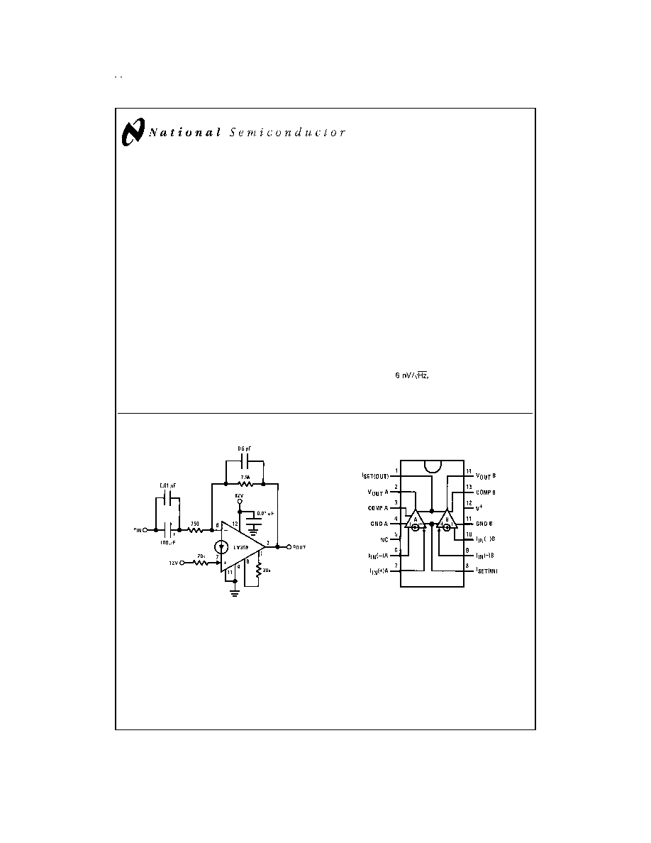
Typical Application
Connection Diagram
DS007788-1
�
A
V
= 20 dB
�
-3 dB bandwidth = 2.5 Hz to 25 MHz
�
Differential phase error
<
1� at 3.58 MHz
�
Differential gain error
<
0.5% at 3.58 MHz
Dual-In-Line Package
DS007788-2
Top View
Order Number LM359J, LM359M or LM359N
See NS Package Number J14A, M14A or N14A
October 1998
LM359
Dual,
High
Speed,
Programmable,
Current
Mode
(Norton)
Amplifiers
� 1999 National Semiconductor Corporation
DS007788
www.national.com
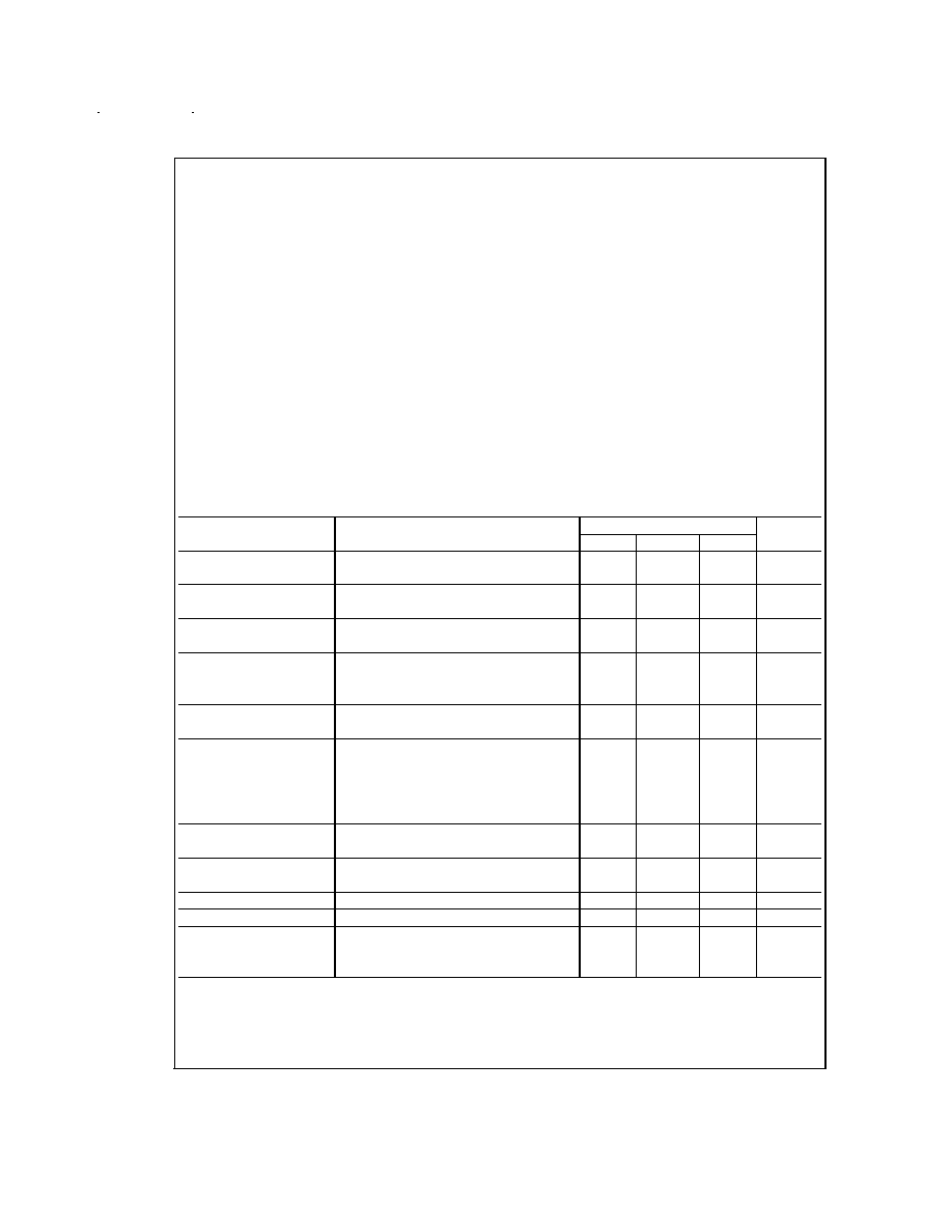
Absolute Maximum Ratings
(Note 1)
If Military/Aerospace specified devices are required,
please contact the National Semiconductor Sales Office/
Distributors for availability and specifications.
Supply Voltage
22 V
DC
or
�
11 V
DC
Power Dissipation (Note 2)
J Package
1W
N Package
750 mW
Maximum T
J
J Package
+150�C
N Package
+125�C
Thermal Resistance
J Package
jA
147�C/W still air
110�C/W with 400 linear feet/min air flow
N Package
jA
100�C/W still air
75�C/W with 400 linear feet/min air flow
Input Currents, I
IN
(+) or I
IN
(-)
10 mA
DC
Set Currents, I
SET(IN)
or I
SET(OUT)
2 mA
DC
Operating Temperature Range
LM359
0�C to +70�C
Storage Temperature Range
-65�C to +150�C
Lead Temperature
(Soldering, 10 sec.)
260�C
Soldering Information
Dual-In-Line Package
Soldering (10 sec.)
260�C
Small Outline Package
Vapor Phase (60 sec.)
215�C
Infrared (15 sec.)
220�C
See AN-450 "Surface Mounting Methods and Their Effect
on Product Reliability" for other methods of soldering
surface mount devices.
ESD rating to be determined.
Electrical Characteristics
I
SET(IN)
= I
SET(OUT)
= 0.5 mA, V
supply
= 12V, T
A
= 25�C unless otherwise noted
Parameter
Conditions
LM359
Units
Min
Typ
Max
Open Loop Voltage
V
supply
= 12V, R
L
= 1k, f = 100 Hz
62
72
dB
Gain
T
A
= 125�C
68
dB
Bandwidth
R
IN
= 1 k
, C
comp
= 10 pF
15
30
MHz
Unity Gain
Gain Bandwidth Product
R
IN
= 50
to 200
200
400
MHz
Gain of 10 to 100
Slew Rate
Unity Gain
R
IN
= 1 k
, C
comp
= 10 pF
30
V/�s
Gain of 10 to 100
R
IN
<
200
60
V/�s
Amplifier to Amplifier
f = 100 Hz to 100 kHz, R
L
= 1k
-80
dB
Coupling
Mirror Gain
at 2 mA I
IN
(+), I
SET
= 5 �A, T
A
= 25�C
0.9
1.0
1.1
�A/�A
(Note 3)
at 0.2 mA I
IN
(+), I
SET
= 5 �A
0.9
1.0
1.1
�A/�A
Over Temp.
at 20 �A I
IN
(+), I
SET
= 5 �A
0.9
1.0
1.1
�A/�A
Over Temp.
Mirror Gain
at 20 �A to 0.2 mA I
IN
(+)
3
5
%
(Note 3)
Over Temp, I
SET
= 5 �A
Input Bias Current
Inverting Input, T
A
= 25�C
8
15
�A
Over Temp.
30
�A
Input Resistance (
re)
Inverting Input
2.5
k
Output Resistance
I
OUT
= 15 mA rms, f = 1 MHz
3.5
Output Voltage Swing
R
L
= 600
V
OUT
High
I
IN
(-) and I
IN
(+) Grounded
9.5
10.3
V
V
OUT
Low
I
IN
(-) = 100 �A, I
IN
(+) = 0
2
50
mV
www.national.com
2
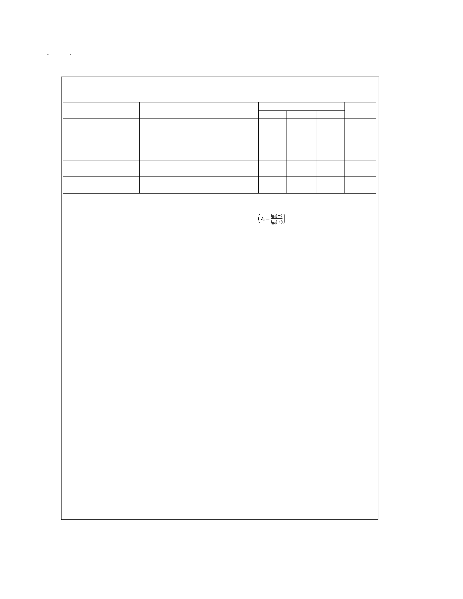
Electrical Characteristics
(Continued)
I
SET(IN)
= I
SET(OUT)
= 0.5 mA, V
supply
= 12V, T
A
= 25�C unless otherwise noted
Parameter
Conditions
LM359
Units
Min
Typ
Max
Output Currents
Source
I
IN
(-) and I
IN
(+) Grounded, R
L
= 100
16
40
mA
Sink (Linear Region)
V
comp
-0.5V = V
OUT
= 1V, I
IN
(+) = 0
4.7
mA
Sink (Overdriven)
I
IN
(-) = 100 �A, I
IN
(+) = 0,
1.5
3
mA
V
OUT
Force = 1V
Supply Current
Non-Inverting Input
18.5
22
mA
Grounded, R
L
=
Power Supply Rejection
f = 120 Hz, I
IN
(+) Grounded
40
50
dB
(Note 4)
Note 1: "Absolute Maximum Ratings" indicate limits beyond which damage to the device may occur. Operating Ratings indicate conditions for which the device is
functional, but do not guarantee specific performance limits.
Note 2: See Maximum Power Dissipation graph.
Note 3: Mirror gain is the current gain of the current mirror which is used as the non-inverting input.
Mirror Gain is the % change in A
I
for two different mirror currents at any given temperature.
Note 4: See Supply Rejection graphs.
www.national.com
3
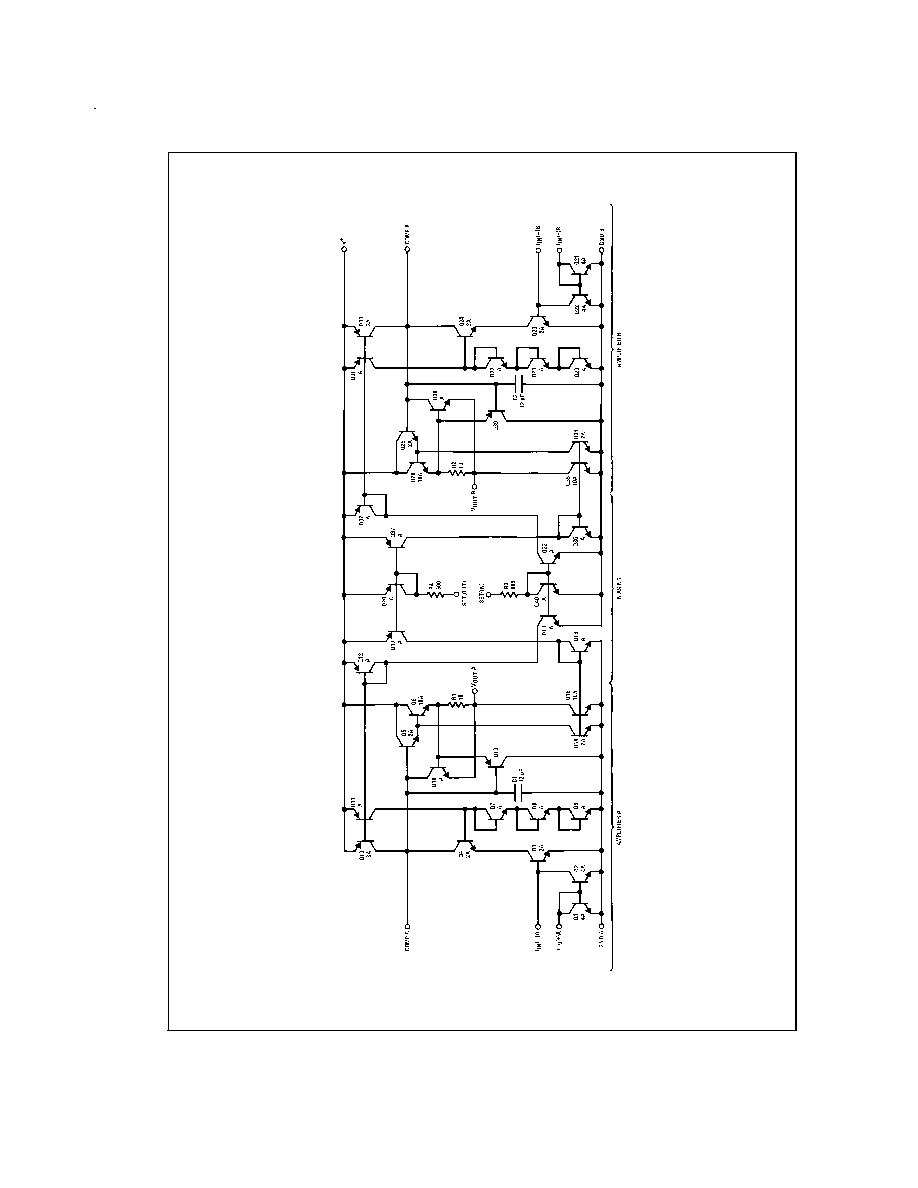
Schematic Diagram
DS007788-3
www.national.com
4
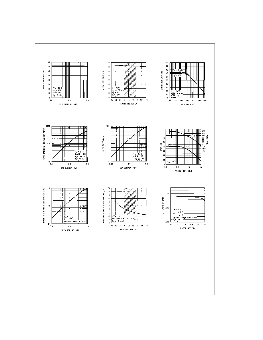
Typical Performance Characteristics
Open Loop Gain
DS007788-39
Open Loop Gain
DS007788-40
Note: Shaded area refers to LM359
Open Loop Gain
DS007788-41
Gain Bandwidth Product
DS007788-42
Slew Rate
DS007788-43
Gain and Phase
Feedback Gain = - 100
DS007788-44
Inverting Input Bias Current
DS007788-45
Inverting Input Bias Current
DS007788-46
Note: Shaded area refers to LM359
Mirror Gain
DS007788-47
www.national.com
5