 | –≠–ª–µ–∫—Ç—Ä–æ–Ω–Ω—ã–π –∫–æ–º–ø–æ–Ω–µ–Ω—Ç: LM3620-8 | –°–∫–∞—á–∞—Ç—å:  PDF PDF  ZIP ZIP |

LM3620
Lithium-Ion Battery Charger Controller
General Description
The LM3620 series of controllers are monolithic integrated
circuits designed to control the charging and end-of-charge
control for lithium-ion rechargeable batteries. The LM3620 is
available in two versions for one or two cell charger applica-
tions. Each version provides the option of selecting the ap-
propriate termination voltage for either coke or graphite an-
ode lithium cells.
The LM3620 can operate from a wide range of DC input
sources (4V to 30V). With no charger supply connected, the
controller draws a quiescent current of only 10nA to minimize
discharging of a connected battery pack.
The LM3620 consists of an operational transconductance
amplifier, a bandgap voltage reference, a NPN driver transis-
tor and precision voltage setting resistors. The output of the
amplifier is made available to drive an external power tran-
sistor if higher drive currents are required.
With a trimmed output voltage regulation of
±
1.2% initial ac-
curacy, the LM3620 provides a simple, precise solution for
end-of-charge control of lithium-ion rechargeable cells.
The LM3620 is packaged in a miniature 5-lead SOT-23 sur-
face mount package for very compact designs.
Features
n
Voltage options for charging 1 or 2 cell stacks
n
Adjustable output voltage for coke or graphite anodes
n
Precision end-of-charge voltage control
n
Wide input voltage range (4V to 30V)
n
Low off state current (
<
10nA)
n
Drive provided for external power stage
n
Tiny SOT-23 package
Typical Application
DS100841-10
July 2000
LM3620
Lithium-Ion
Battery
Charger
Controller
© 2000 National Semiconductor Corporation
DS100841
www.national.com
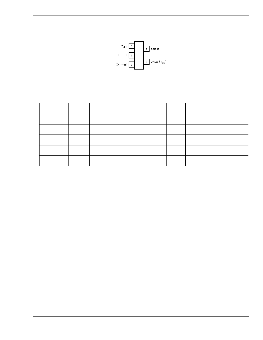
Connection Diagram
Ordering Information
Device Order
Number
Package
Marking
Output
Voltage
Initial
Accuracy
(25∞C)
Over
Temperature
Accuracy
(0 to 70∞C)
Number
of Cells
Supplied as
LM3620M5-4
D10B
4.1V/4.2V
1.2%
2%
1
1000 Unit increments on Tape and
Reel
LM3620M5X-4
D10B
4.1V/4.2V
1.2%
2%
1
3000 Unit increments on Tape and
Reel
LM3620M5-8
D11B
8.2V/8.4V
1.2%
2%
2
1000 Unit increments on Tape and
Reel
LM3620M5X-8
D11B
8.2V/8.4V
1.2%
2%
2
3000 Unit increments on Tape and
Reel
The small physical size of the SOT23-5 Package does not allow for the full part number marking. Devices will be marked with the
designation shown in the column Package Marking.
The devices are shipped in tape-and-reel format. The standard quantity is 250 units on a reel (indicated by the letters "M5" in the
part number), or 3000 units on a reel (indicated by the letters "M5X" in the part number).
5-Lead SOT23-5 Surface Mount Package
DS100841-1
Refer to the Ordering Information Table in
this Data Sheet for Specific Part Number
See NS Package MF05A
LM3620
www.national.com
2
Absolute Maximum Ratings
(Note 1)
If Military/Aerospace specified devices are required,
please contact the National Semiconductor Sales Office/
Distributors for availability and specifications.
Input Voltage (V
DRIVE
)
35V
V
EXT
1.5V
Junction Temperature
150∞C
Storage Temperature
-65 to +150∞C
Lead Temp. Soldering
Vapor Phase (60 sec.)
Infrared (15 sec.)
215∞C
220∞C
Power Dissipation (T
A
= 25∞C)
(Note 2)
300mW
ESD Susceptibility (Note 3)
2000V
Operating Ratings
(Note 1)
Ambient Temp. Range
0∞C to 70∞C
Junction Temp. Range
0∞C to 125∞C
Thermal Resistance (Junction to
Ambient,
J-A
)
280∞C/W
Input Voltage (V
DRIVE
)
4V to 30V
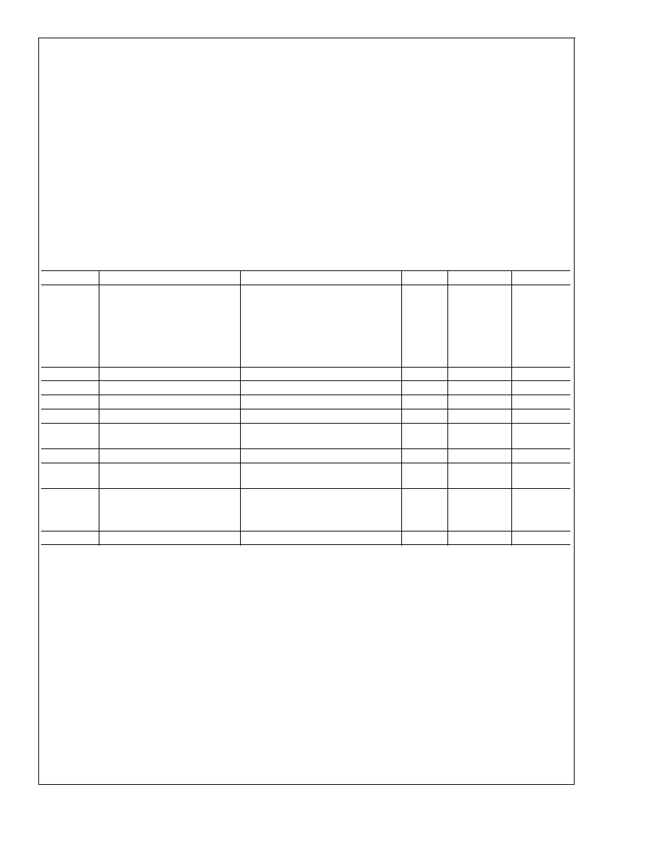
Electrical Characteristics
LM3620-4
V
DRIVE
= 5V, I
DRIVE
= 2mA. Limits with boldface type apply over the full operating ambient temperature range, 0∞C to +70∞C,
limits with standard typeface apply for T
A
= 25∞C.
Symbol
Parameter
Conditions
Typical
Limit
Units
V
REG
Regulated Output Voltage (pin
1 to ground)
Pin 5 shorted to pin 1 (graphite
anode)
4.1
4.051/4.018
V(min)
4.149/4.182
V(max)
Pin 5 open (coke anode)
4.2
4.150/4.116
V(min)
4.250/4.284
V(max)
Regulated Output Voltage
Tolerance
Either Pin 5 setting
±
1.2/
±
2.0
%
V
REG
/V
DRIVE
Supply Sensitivity
V
REG
for 5V
V
DRIVE
30V
100
µV/V(max)
I
Q
Quiescent Current
V
REG
= 4.5V, V
EXT
= 1.0V (Note 4)
400
750
µA(max)
I
OFF
Off State Current
V
DRIVE
open circuited (Note 5)
10
200
nA(max)
I
DRIVE
Drive Pin Sink Current
V
DRIVE
= 5.0V
20
15
mA(min)
Gm
(DRIVE)
Drive Pin Transconductance
I
DRIVE
/
V
REG
2mA
I
DRIVE
15mA
3
A/V
I
EXT
External Pin Source Current
V
EXT
= 1V (Note 6)
3
2.5
mA(min)
Gm
(EXT)
External Pin Transconductance
I
EXT
/
V
REG
, V
EXT
= 1V
0mA
I
EXT
2.5mA
0.8
A/V
R
IN
V
REG
Input Resistance
Pin 1 to Ground.
Circuit biased with V
DRIVE
applied
V
DRIVE
open circuited
46
k
42
M
R
F
Feedback Resistance
Pin 1 to Pin 5
1500
LM3620
www.national.com
3

LM3620-8
V
DRIVE
= 5V, I
DRIVE
= 2mA. Limits with boldface type apply over the full operating ambient temperature range, 0∞C to + 70∞C,
limits with standard typeface apply for T
A
= 25∞C.
Symbol
Parameter
Conditions
Typical
Limit
Units
V
REG
Regulated Output Voltage (pin
1 to ground)
Pin 5 shorted to pin 1 (graphite
anode)
8.2
8.102/8.036
V(min)
8.298/8.364
V(max)
Pin 5 open (coke anode)
8.4
8.299/8.232
V(min)
8.501/8.568
V(max)
Regulated Output Voltage
Tolerance
Either Pin 5 setting
±
1.2/
±
2.0
%
V
REG
/V
DRIVE
Supply Sensitivity
V
REG
for 5V
V
DRIVE
30V
200
µV/V(max)
I
Q
Quiescent Current
V
REG
= 8.7V, V
EXT
= 1.0V (Note 4)
400
750
µA(max)
I
OFF
Off State Current
V
DRIVE
open circuited (Note 5)
10
200
nA(max)
I
DRIVE
Drive Pin Sink Current
V
DRIVE
= 5.0V
20
15
mA(min)
Gm
(DRIVE)
Drive Pin Transconductance
I
DRIVE
/
V
REG
2mA
I
DRIVE
15mA
1.5
A/V
I
EXT
External Pin Source Current
V
EXT
= 1V (Note 6)
3
2.5
mA(min)
Gm
(EXT)
External Pin Transconductance
I
EXT
/
V
REG
, V
EXT
= 1V
0mA
I
EXT
2.5mA
0.4
A/V
R
IN
V
REG
Input Resistance
Pin 1 to Ground.
Circuit biased with V
DRIVE
applied
V
DRIVE
open circuited
110
k
42
M
R
F
Feedback Resistance
Pin 1 to Pin 5
2900
Note 1: Absolute Maximum Ratings indicate limits beyond which damage to the device may occur. Operating Ratings indicate conditions for which the device is in-
tended to be functional, but do not guarantee specific performance limits. For guaranteed specifications and test conditions, see the Electrical Characteristics.
Note 2: The maximum power dissipation must be derated at elevated temperatures and is limited by T
JMAX
(maximum junction temperature),
J-A
(junction-to-ambient thermal resistance) and T
A
(ambient temperature). The maximum power dissipation at any temperature is: PDiss
MAX
= (T
JMAX
- T
A
)/
J-A
up to
the value listed in the Absolute Maximum Ratings.
Note 3: Rating is for the human body model, a 100 pF capacitor discharged through a 1.5k
resistor into each pin.
Note 4: Quiescent current is all current flowing to ground when the voltage at the V
REG
pin is forced to be above the nominal regulating voltage (V
REG
).
Note 5: Off current is all of the current flowing to ground including all leakage current that would be drawn from the battery connected to the V
REG
terminal.
Note 6: When the External pin is being used as the driving source, it is recommended to keep the operating point of V
EXT
1V. If greater than 1V, the internal circuitry
would bias I
DRIVE
to conduct up to the current limit level continuously causing unnecessary power dissipation in the device.
LM3620
www.national.com
4
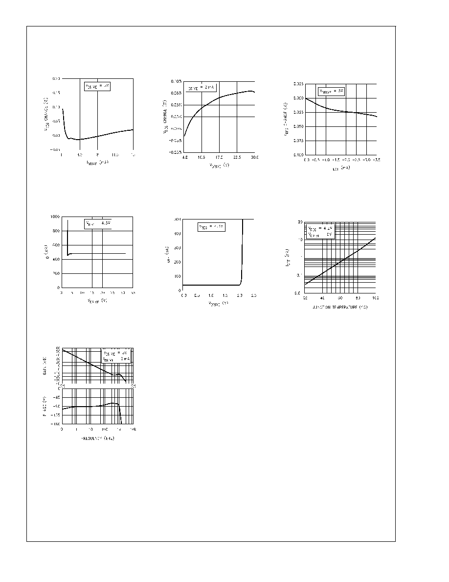
Typical Performance Characteristics
Unless otherwise specified, T
A
= 25∞C.
LM3620M5-4
Normalized Regulation Voltage
Change vs I
DRIVE
DS100841-4
LM3620M5-4
Normalized Regulation Voltage
Change vs V
DRIVE
DS100841-8
LM3620M5-4
Normalized Regulation Voltage
Change vs I
EXT
DS100841-7
LM3620M5-4
Quiescent Current
vs V
DRIVE
DS100841-5
LM3620M5-4
Off State Current vs V
DRIVE
DS100841-6
LM3620M5-4
Off State Current
vs Temperature
DS100841-3
LM3620M5-4
Bode Plot (
V
DRIVE
/
V
REG
)
DS100841-9
LM3620
www.national.com
5