 | –≠–ª–µ–∫—Ç—Ä–æ–Ω–Ω—ã–π –∫–æ–º–ø–æ–Ω–µ–Ω—Ç: LM3641 | –°–∫–∞—á–∞—Ç—å:  PDF PDF  ZIP ZIP |
LM3641
Lithium-Ion Battery Pack Protection Circuit
General Description
The LM3641 Lithium Protection Integrated Circuit resides in-
side a 3.6V Lithium-Ion battery pack consisting of a single
cell or multiple parallel cells. The IC controls the ON/OFF
state of a pair of low threshold N-channel power MOSFETs
placed in series with the battery cell(s). The purpose of this
MOSFET pair is to protect the cell(s) from inadvertent elec-
trical over-stress. The IC compares the cell voltage against
internally programmed minimum and maximum limits. Tran-
sient voltage faults of approximately 1.25 seconds are toler-
ated.
The IC also monitors the bi-directional current flow in the bat-
tery pack by measuring the voltage across a robust 4 m
current sensing resistor internal to the protection IC pack-
age. The IC turns OFF the MOSFET pair whenever any fault
limit is exceeded. Momentary current surges
<
4 ms are tol-
erated.
The Enable pin allows external ON/OFF control of the MOS-
FET pair and resets the IC after the MOSFET pair is turned
OFF and the pack is safe to operate again.
The limits for overcharge and overdischarge voltage, as well
as independent limits for each direction of overcurrent are
factory adjusted employing EEPROM.
Features
n
Automatic battery disconnect when the cell is
over-charged or over-discharged.
n
Maximum cell voltage for MOSFET conduction is factory
programmable between 4.0V and 4.4V with a
±
25 mV
tolerance (0∞C to +60∞C).
n
Minimum cell voltage for MOSFET conduction =
0.57
∑V
MAX
±
3.5% (0∞C to +60∞C).
n
Internal 4 m
current sense resistor provides
±
0.5A
maximum accuracy for detection of overcurrent faults.
The maximum charge and discharge current is factory
programmable between 1A and 5A. A single overcurrent
fault event opens and protects the MOSFET pair.
n
Automatic detection of safe pack conditions for recovery
(MOSFET pair ON) from a fault condition (over/under
discharged or overcurrent).
n
Average current drain = 1.2 µA typical.
n
Optional Enable pack terminal can be used to prevent
accidental short circuit of pack and for maximizing the
shelf life of the pack (IC powers down when the pack is
not in use).
n
Over-current events cause connection of an internal
50 k
"FET-Bypass" resistance across OFF MOSFET
pair. Loads
>
3≠7 M
are required for return to
conduction mode.
n
Over-charged states cause connection of a 5 k
"Cell-Bypass" resistor to ensure that the cell is not
allowed to be overcharged by leakage paths.
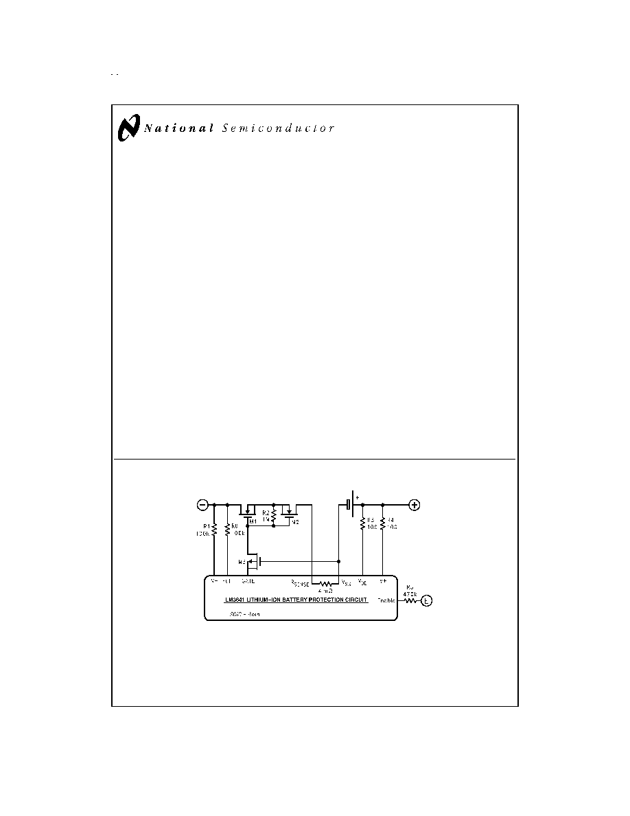
Typical Application
TRI-STATE
Æ
is a registered trademark of National Semiconductor Corporation.
DS012931-1
January 1999
LM3641
Lithium-Ion
Battery
Pack
Protection
Circuit
© 1999 National Semiconductor Corporation
DS012931
www.national.com
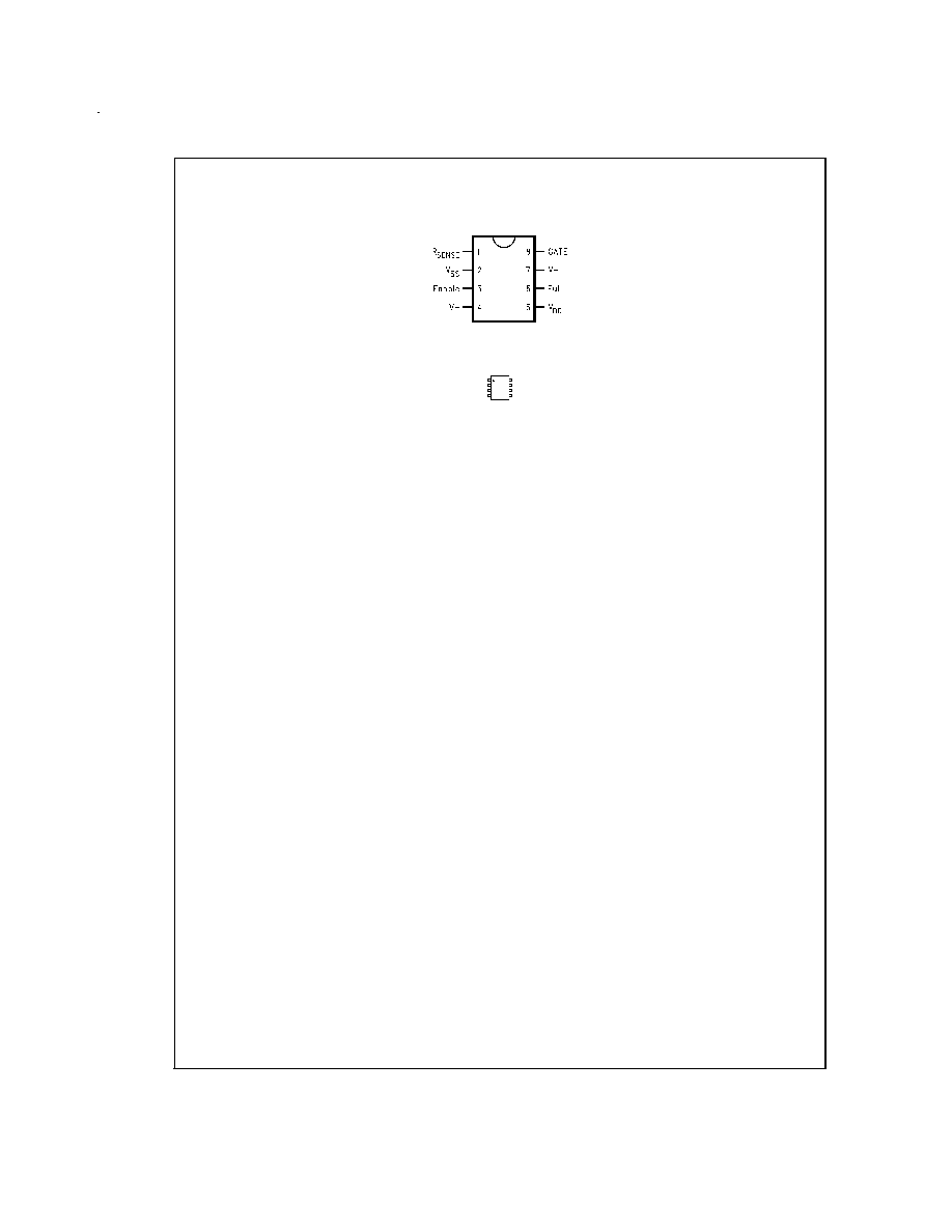
Connection Diagram and Ordering Information
Top View
8-Lead SOIC (M08A)
DS012931-2
Actual Size
DS012931-3
Order Number LM3641M
See NS Package Number M08A
This device is factory programmable. Contact your local NSC sales office for ordering information.
www.national.com
2

Absolute Maximum Ratings
(Note 1)
If Military/Aerospace specified devices are required,
please contact the National Semiconductor Sales Office/
Distributors for availability and specifications.
Maximum Input Supply Voltage
(V
DD
)
-0.3V to 5.5V
V+ or GATE or Full Pin Voltage
-0.3V to V
DD
+ 0.3V
Enable or V- Pin Current
±
200 µA
Power Dissipation (Note 2)
Internally limited
ESD Susceptibility
Human Body Model (Note 3)
2 kV
Lead Temperature
(Soldering, 10s)
260∞C
Operating Range
(Note 1)
Ambient Temperature Range
0∞C to +60∞C
Junction Temperature Range
-40∞C to +125∞C
LM3641
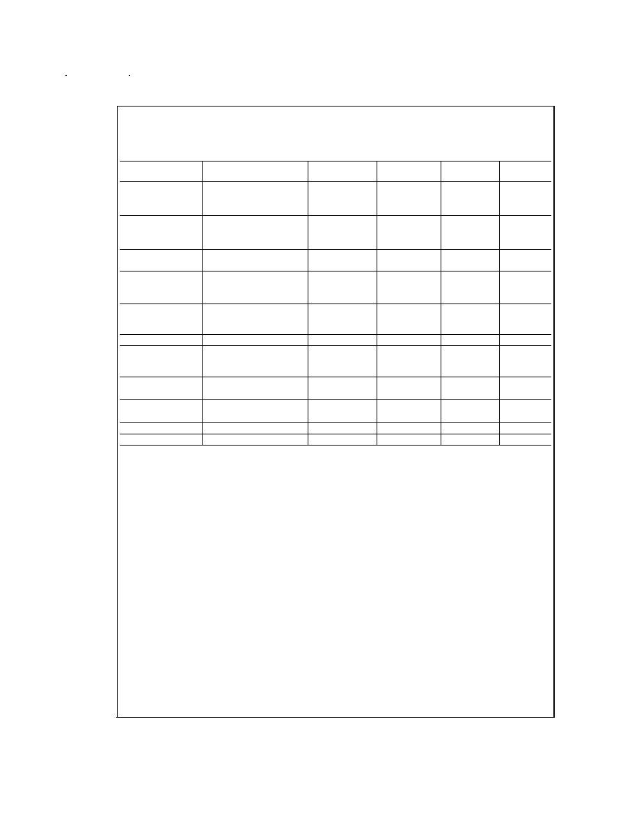
Electrical Characteristics
Specifications with standard type face for T
J
= 25∞C, and those with bold type apply over full Operating Temperature Range.
Unless otherwise specified, V
SS
= 0V, V
DD
= 3.6V, V
ENABLE
= V
DD
.
Symbol
Parameter
Conditions
Typical
(Note 4)
Limit
(Note 5)
Units
V
MAX
Overcharge Protection
Accuracy
0∞C to +60∞C
A.S.(Note 6)
±
25
V
mV(max)
V
MAX-85
Overcharge Protection
Accuracy
Temp = 85∞C
<
V
MAX
@
25∞C
V
MAX-RANGE
Overcharge Protection
Program Range
4.2
V
4.0
V(max)
4.4
V(min)
V
SAFE
Max Cell Voltage Overshoot
(referred to V
MAX
)
V
MAX
+ 100 mV
V
V
MIN
Overdischarge Protection
Accuracy
0.57
∑V
MAX
V
+0.04
∑ V
MAX
V(max)
-0.04
∑ V
MAX
V(min)
V
GATE-FETS-ON
Gate Pin High
1 M
Load
V
DD
-50 mV
V
I
GATE-FETS-ON
Gate Pin FET Turn-on
Impedence
2
k
I
GATE-FETS-OFF
Gate Pin OFF Current
V
Gate
= 0V
10
nA
I
MAX-CHG
Overcurrent Protection
Accuracy -- Charging
A.S.(Note 6)
A
+0.5
A(max)
-0.5
A(min)
I
MAX-DIS
Overcurrent Protection
Accuracy -- Disharging
A.S.(Note 6)
+0.5
-0.5
A
A(max)
A(min)
I
SUPPLY
Supply Current (V
DD
, V+,
control pins) (Note 7)
normal mode
V
DD
= 3.6V
excludes I
R2
120
1
4
µApeak
µA rms
µA rms(max)
I
ENABLE PIN
Enable Pin Current (sink)
V
ENABLE
= V
DD
400
nA
I
V+
Cell Sense Pin Current (sink)
V
DD
= 3.6V
40
nA rms
t
SAMPLE
Cell Voltage Sampling
Period -- Normal and
Overdischarge Modes
V+
<
V
MAX
1
s
0.75
s(min)
1.5
s(max)
t
SAMPLE-OVERCHARGED
Cell Voltage Sampling
Period -- Overcharged
V+
>
V
MAX
0.25
s
0.19
s(min)
0.28
s(max)
N
SAMPLE
Number of consecutive
samples for overcharge or
overdischarge prior to
disconnect
4
www.national.com
3
LM3641
Electrical Characteristics
(Continued)
Specifications with standard type face for T
J
= 25∞C, and those with bold type apply over full Operating Temperature Range.
Unless otherwise specified, V
SS
= 0V, V
DD
= 3.6V, V
ENABLE
= V
DD
.
Symbol
Parameter
Conditions
Typical
(Note 4)
Limit
(Note 5)
Units
t
OVERCHARGE
Overcharge Transient
Rejection Time (Note 8)
1.6
s
0.57
s(min)
2.64
s(max)
t
OVERDISCHARGE
Overdischarge Transient
Rejection Time (Note 8)
4
s
3
s(min)
6
s(max)
t
OVERCURRENT
Overcurrent Transient
Rejection Time
6
ms
DC
Duty Cycle of Pulse Charging
V
MAX
<
V
CELL
<
V
SAFE
87.5
%
V
CELL
>
V
SAFE
50
%
t
ENABLE-DELAY
Delay from Rising/Falling
Enable pin to FETs ON/OFF
(Note 9)
L
H
H
L
5
3
ms
V
RECOVERY
MOSFET Threshold Voltage
±
36
mV
V
MIN-CHARGE
Minimum Cell Voltage that
can be charged, V
GATE
V
DD
(Note 10)
0
V
V
FULL-HIGH
Maximum High Output
Voltage of Full Pin
V+
>
V
MAX
V
DD
- 1.2V
I
FULL
<
4 µA
I
FULL-OFF
Source/Sink Current of Full
Pin in TRI-STATE
Æ
V+
<
V
MAX
10
nA
V
FULL
= 0V
I
R-SENSE
Maximum R
SENSE
Current
Duration
<
6 ms
60
A
R
SENSE
R
SENSE
Range
4
m
Note 1: Absolute Maximum ratings indicate limits beyond which damage to the device may occur. Operating Ratings indicate conditions for which the device is in-
tended to be functional, but do not guarantee specific performance limits. For guaranteed specifications and test conditions, see Electrical Characteristics. The guar-
anteed specifications apply only for the test conditions listed. Some performance characteristics may degrade when the device is not operated under the listed test
conditions.
Note 2: The maximum allowable power dissipation is calculated by using P
DMAX
= (T
JMAX
- T
A
)/
JA
, where T
JMAX
= 150∞C, T
A
is the ambient temperature, and
JA
= 160∞C/W.
Note 3: The human body model is a 100 pF capacitor discharged through a 1.5 k
resistor into each pin.
Note 4: Typical numbers are at 25∞C and represent the most likely parametric norm.
Note 5: Limits are 100% production tested at 25∞C. Limits over the operating temperature range are guaranteed through correlation using Statistical Quality Control
(SQC) methods. The limits are used to calculate National's Averaging Outgoing Quality Level (AOQL).
Note 6: Application Specific. This analog parameter's value is programmed during National's production testing of the device. Please contact your local NSC sales
office to specify the V
MAX
, I
MAX-CHG
and I
MAX-DIS
values when ordering this device. V
MAX
can be programmed between 4.0V and 4.4V. I
MAX-CHG
can be programmed
between 1A and 5A. I
MAX-DIS
can be programmed between 1A and 5A.
Note 7: I
SUPPLY
includes V
DD
pin peak currents that occur at each t
sample
period. The I
DD
peak current duration is approximately 2.2 ms and the I
VDD
peak current
is approximately 120 µA.
Note 8: Computed from 4 sample periods of the worst case values of t
SAMPLE
and t
SAMPLE-OVERCHARGED
.
Note 9: High pulses
<
3 ms (typ) will be typically ignored and low pulses
<
5 ms (typ) will be typically ignored.
Note 10: V
MIN-CHARGE
will be limited by the threshold of M3.
www.national.com
4
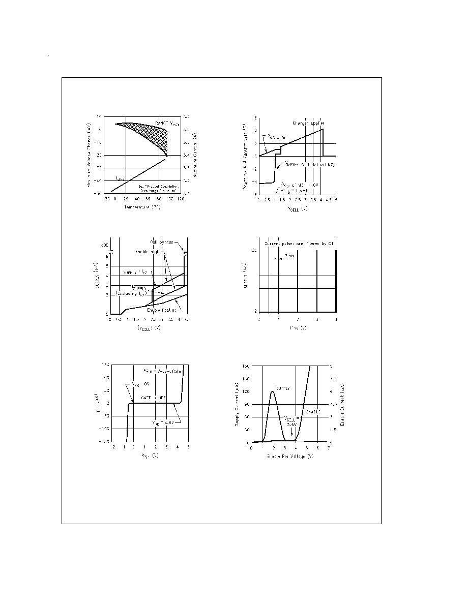
Typical Performance Characteristics
Maximum Current and Normalized
Maximum Voltage vs. Temperature
DS012931-4
GATE Pin and MOSFET GATE
Voltage vs CELL Voltage
DS012931-5
Supply Current
DS012931-6
Supply Current vs Time
DS012931-7
Pin* Current vs
Pin* Voltage
DS012931-8
Supply and Enable Current
vs Enable Voltage
DS012931-9
www.national.com
5
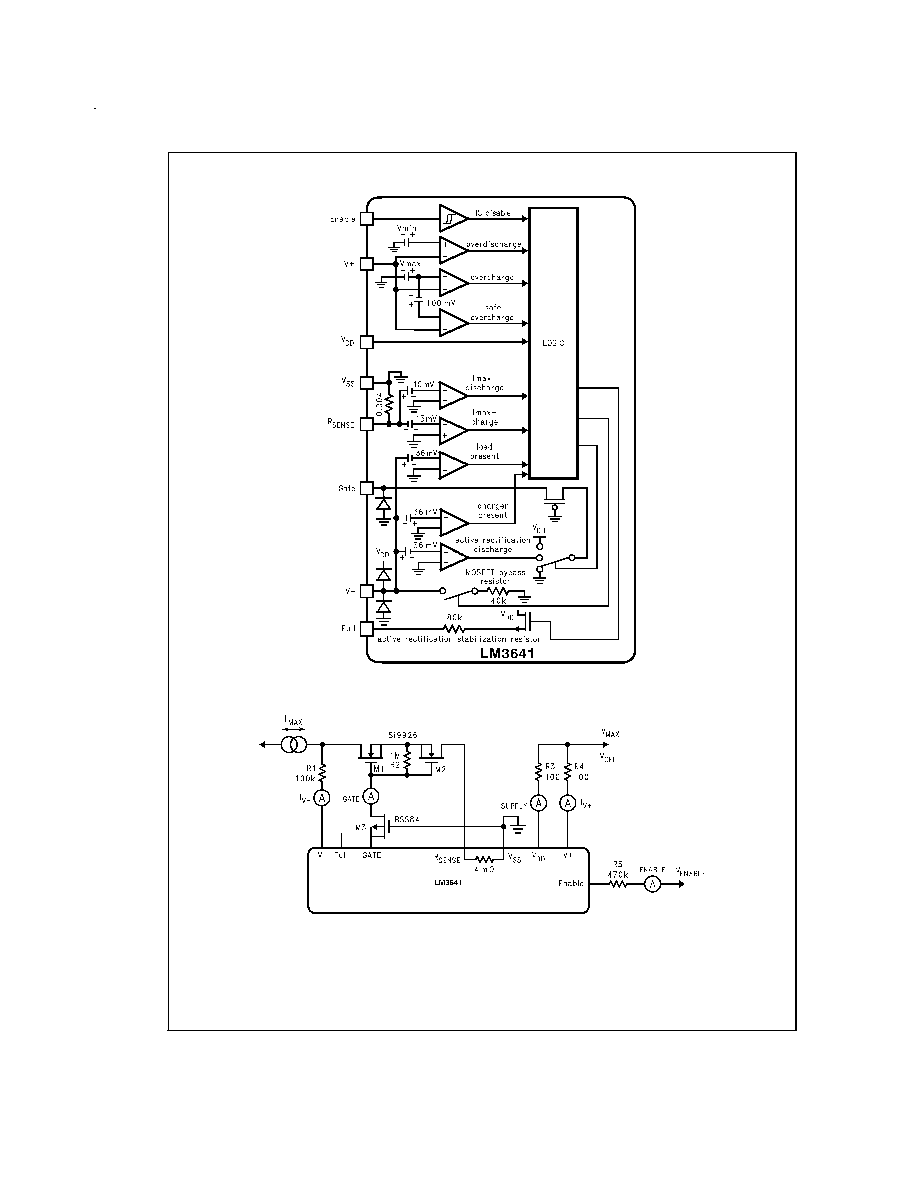
Block Diagram
Test Circuit
DS012931-10
DS012931-11
www.national.com
6

Product Description
Normal charging of Li-Ion packs requires Constant Voltage
Constant Current (CVCC) chargers that terminate charging
at a voltage value just below the maximum protection volt-
age (V
MAX
). Only in the event of an invalid charger or an out
of compliance charger operation should the protection IC ter-
minate charging.
OVERCHARGE PROTECTION
The IC protects the cell(s) against overcharge. Normally, the
cell voltage is sampled once a second. Four consecutive
samples of V
CELL
>
V
MAX
result in the MOSFET pair turning
OFF. The transient response for overvoltage requires one
sample at the t
SAMPLE
period (1s typical) and three t
SAMPLE-
OVERVOLTAGE
periods (0.25s typical). The first overcharge
event is asynchronous to the 1 second sampling so the delay
between the actual instance of overcharge and the first
sample can result anywhere in the range of zero to t
SAMPLE
.
The requirement for 4 consecutive samples of V
CELL
>
V
MAX
filters noise from the cell due to transient currents. Should
the cell voltage exceed V
MAX
by more than 100 mV (V
SAFE
),
the MOSFETs will turn off on the first sample reading. This
provides an extra measure of safety. The return to conduc-
tion mode requires that a load be applied to the pack or
V
CELL
<
V
MAX
- 20 mV. Also a L
H signal on the Enable pin
will reset the GATE high, but if V
CELL
>
V
MAX
, the GATE will
go low again after 1.75 seconds. Whenever an overcharge
disconnect has occurred, a cell bypass resistor (
5 k
) is
switched across the V
DD
and V
SS
pins and the Full pin pulls
to near V
DD
. The cell bypass resistor ensures that the cell is
discharged even though some component of R1's current
will still flow in the cell, if a charger is applied. The cell by-
pass resistor is removed when V
CELL
<
V
MAX
again.
ACTIVE RECTIFICATION
Overcharged cells can be discharged by the application of a
load to the pack. Active Rectification is the biasing of the
power MOSFETs GATE so that the V
DS
= V
RECOVERY
for dis-
charge currents. The MOSFETs turn OFF for charge cur-
rents. The Active Rectification amplifier assures uninter-
rupted conduction for discharge currents only. The Full pin's
output impedance is
80 k
when active high (V
CELL
>
V
MAX
) and TRI-STATE when inactive (V
CELL
<
V
MAX
). The
Full pin can optionally supply a small FET current necessary
to stabilize the Active Rectification loop by maintaining at
least (V
DD
-1V)/R6+80k)
∑I
D
in the MOSFET. The Full pin's
overcharge signal could be used in applications where the
charger is logically disabled by the protection circuit, a
change time-out circuit is initiated or whenever an over-
charge signal is otherwise desired. The Full signal will go low
(TRI-STATE with an external resistor pulldown) and cell by-
pass turns off if a cell decays to V
CELL
<
V
MAX
.
OVERDISCHARGE PROTECTION
The cell(s) are also protected against overdischarge. Four
consecutive 1 Hz samples of V
CELL
<
V
MIN
result in the
MOSFET pair turning OFF. Cells that have discharged below
V
MIN
due to long periods of self-discharge can still be
charged. Return to conduction mode for overdischarged
packs automatically occurs if a charger is applied to the
pack. Also a L
H signal on the Enable pin will reset the
GATE high, however if V
CELL
<
V
MIN
, the GATE will turn
OFF again in 4 seconds.
OVERCURRENT PROTECTION
The battery current is monitored continuously by measuring
the voltage across the internal sense resistor. If the terminal
current exceeds I
MAX-CHG
(programmable) in the charge
mode for longer than t
OVERCURRENT
, the MOSFET pair dis-
connects. Similarly, if the terminal current exceeds I
MAX-DIS
(programmable) in the discharge mode for longer than
t
OVERCURRENT
, the MOSFET pair disconnects. Recovery to
conduction mode requires either 1) a momentary detach-
ment of the pack so the Enable pin can be cycled low, then
high or 2) a direct low to high signal to the Enable pin con-
trolled from logic.
ENABLE PIN
The pack can be protected from accidental short circuits
should the Enable pin be made available as a third battery
pack terminal. This third pack terminal is tied to the pack's
positive terminal through a connection on either a valid
charger or load. Shorting the high impedance Enable pin to
the pack's positive terminal enables all functions of the pro-
tection circuit. The Enable pin disables the MOSFET pair
whenever this pin is floating, such as when the battery pack
is detached from a valid load or charger. Floating the Enable
pin also forces the protection circuit into FET's OFF mode to
maximize the shelf life of the battery pack. When the Enable
pin is used to recover from overcharge, overdischarge or
overcurrent events, the voltage measurement system
memory is cleared of previous results. If the MOSFET by-
pass resistor is active, and the Enable goes low, the bypass
resistor turns OFF. A series resistor of 470 k
to 1 M
be-
tween the Enablel terminal of the pack and the Enable pin of
the IC, protects the IC from ESD events at the pack's termi-
nals.
SLEEPMODE
Sleepmode is a reduced current state that occurs when the
Enable pin is floating or low. The FETs are turned OFF.
Sleepmode minimizes the artificial self-discharge of the pack
when the pack is not in use.
INVALID CHARGER
Assume a charger that exceeds the V
MAX
rating of the IC is
applied to the pack. The power MOSFETs will eventually turn
OFF due to overcharge if I
CHARGER
<
I
MAX-CHG
, or turn OFF
due to overcurrent if the invalid charger's current exceeds
I
MAX-CHG
. If the charger was applied to the pack with the po-
larity reversed, then the MOSFETs would eventually turn
OFF due to either overdischarge or overcurrent depending
on the magnitude of the charger's available current. In either
case, the voltage on the V- pin will be driven by the open cir-
cuit voltage of the charger. The V- pin is clamped by internal
diodes to V
DD
and V
SS
and the pin's current limited by R1
(see the typical curve "Pin Current vs. Pin Voltage") with R1
= 100k, the pin current will not exceed the maximum recom-
mended value of
±
200 µA for a
±
20V invalid charger. Higher
invalid charger voltages can be tolerated when using higher
values for R1. Proper LCCE operation is not limited, even by
values for R1 in excess of 1 M
.
www.national.com
7
Product Description
(Continued)
NORMAL TERMINATION OF CHARGING
As you can see in
Figure 1, the cell voltage must exceed
V
MAX
for 4 consecutive samples before the MOSFET pair is
turned OFF (1). Once V
MAX
is exceeded, the sampling rate
increases to 4 Hz. The sampling rate will return to 1 Hz only
after 4 consecutive samples result in V
CELL
<
V
MAX
. After
the MOSFET pair is OFF (2), the voltage across the cell(s)
relax and the cell voltage will drop below V
MAX
. On the next
sample, (3), the MOSFET pair will turn ON. As long as the
charger is applied and the MOSFET pair turn ON, the cell
voltage will exceed V
MAX
again. The cycle of 4 samples ON
a 1 samples OFF will continue until the cell voltage equals
V
MAX
after the MOSFET pair is OFF, (4). This example exag-
gerates the rate of these events. The actual operation would
result in many ON/OFF cycles at a decreasing duty cycle
prior to complete termination of charge. The cell bypass re-
sistor will discharge the cell enough to turn on the GATE over
a period of minutes.
NORMAL TERMINATION OF DISCHARGING
The cell voltage must go below V
MIN
for 4 consecutive
samples before the MOSFET pair is turned OFF (1), which is
shown in
Figure 2. Once the MOSFET pair is OFF and the
current is interrupted, the voltage across the cell(s) will in-
crease and the cell voltage could exceed V
MIN
(2). The
MOSFET pair remain off until a charger is applied to the
pack (3). The presence of a charger turns the MOSFET pair
ON. Deeply discharged cells will be charged, although for
some narrow bands of V
CELL
, the GATE may occasionally
pulse OFF momentarily.
TERMINATION OF ILLEGALLY HIGH CHARGING
Should a high charge current be applied to the pack near the
end of charge, the cell voltage could exceed V
SAFE
, which is
approximately 100 mV greater than V
MAX
(1), see
Figure 3.
On the first detection of a cell voltage in excess of V
SAFE-
OVERCHARGE
, the MOSFET pair will be turned OFF (2). The
sample rate increases to 4 Hz after the first detection of
V
CELL
>
V
MAX
. It is desirable under these circumstances for
the MOSFET pair to turn ON for only the shortest allowed
time period, which is 0.25 seconds. Each sample exceeding
V
SAFE
causes the MOSFET pair to turn OFF (3). Should the
cell voltage not drop below V
MAX
after the MOSFET pair turn
OFF, the MOSFET pair remain OFF (4). This example exag-
gerates the rate of these events. The actual operation would
result in many ON/OFF cycles at a decreasing duty cycle
prior to complete termination of charge.
LOAD APPLIED IN OVERCHARGED STATE
If a load is momentarily applied while the cell is in over-
charged state, then the MOSFET pair is momentarily turned
ON, see
Figure 4. The MOSFET pair will stay ON only as
long as the load is applied. The MOSFET pair will stay ON
after the load is removed only if the cell voltage remains be-
low V
MAX
for 4 consecutive samples. Possible events are
shown as examples of operation:
(1) A momentary load is applied to an overcharged cell, the
MOSFET pair stay ON only as long as the load is applied.
The gate drive is limited so that the MOSFET pair ON volt-
age will match a bias voltage generated internal to the IC,
V
RECOVERY
. This bias voltage is the minimum MOSFET ON
voltage that allows for the detection of a load. This mode of
operation is
Active Rectification. Note that the MOSFET pair
do not turn ON for the momentary application of a charger.
(2) A load is applied for less than 4 samples. The MOSFET
pair is ON for the load period, but turn OFF after the load is
removed. Only after the 4th sample of V
CELL
<
V
MAX
will the
MOSFET pair turn ON, this time will full drive potential.
(3) Assume the application of a charger. Conduction is al-
lowed because the FETs are ON, but the MOSFET pair will
stay ON only for 4 consecutive overcharge samples. See the
diagram for the "Normal Termination of Charging".
(4) The MOSFET pair will turn OFF after the 4 consecutive
overcharge samples.
(5) A load is applied and after V
CELL
<
V
MAX
for 4 consecu-
tive samples, the MOSFET pair turn ON full. As long as
V
CELL
stays below V
MAX
, the MOSFET pair will stay ON.
Should a load be applied that exceeds the overcurrent-
discharge current limit while the IC is in active rectification
mode, the MOSFET pair will turn OFF. Recovery requires
that either the IC detects a load greater than 3≠7 M
or that
the cell voltage remains under V
MAX
for 4 samples. If the
load that caused overcurrent remains after the cell voltage
drops under V
MAX
for 4 samples, then the MOSFET pair will
turn ON once more and normal overcurrent mode is entered.
DS012931-12
FIGURE 1. Normal Termination of Charging
www.national.com
8
Product Description
(Continued)
Fail Safe Features
The safety provided by the LM3641 goes beyond the normal
operation of the IC. The design of the IC includes many as-
pects that continue to assure protection of the cells even
when malfunctions occur.
∑
A rugged internal sense resistor offers precise overcur-
rent response (magnitude and time) which allows smaller
volume power MOSFETs to be used. If the internal resis-
tor's sense circuitry's input open circuit (very unlikely),
the MOSFET pair will turn OFF. The IC will fail safe.
∑
If any pin becomes detached from the PCB, either the
MOSFETs will turn OFF or the part will continue to protect
the Cell.
∑
The maximum cell voltage limit is trimmed by EEPROM
and offers optimal accuracy. Each EEPROM cell has re-
dundant EEPROM transistors for additional reliability.
The EEPROM register also contains a parity check bit. In
the rare event that an EEPROM bit would change state,
the power MOSFETs will be turned OFF rather than allow
the IC to operate out of specification.
∑
The external MOSFETs are specified to provide ad-
equate illegal charger withstand capability. Because of
M3, the IC is designed to never be exposed to more than
the actual cell voltage. Therefore the IC's maximum rated
supply voltage does not limit the magnitude of illegal
charger voltages that can be protected by the IC. M3's Vt
also guarantees that shorted cells can not be charged.
DS012931-13
FIGURE 2. Normal Termination of Discharging
DS012931-14
FIGURE 3. Termination of Illegally High Charging
DS012931-15
FIGURE 4. Load Applied in Overcharged State
www.national.com
9
Fail Safe Features
(Continued)
∑
In the event of an extremely high charge current, the cell
voltage could exceed the maximum supply rating of the
IC. The IC is protected by internal voltage clamps and the
external 100
resistors R3 and R4.
∑
The external MOSFET pair turn-off resistor R2 aids in fail
safe operation in the rare event that the IC fails. Dual in-
dependently controlled series switches internal to the IC
must both turn on to allow the MOSFET pair to conduct.
If either control signal is in error, the external resistor R2
will ensure that the MOSFET pair turn OFF.
∑
The LM3641 is 100% tested for all aspects of operation.
The digital design-for-test methodology allows the cir-
cuitry to be tested at a greatly accelerated rate while
maintaining near perfect fault coverage.
∑
The cell bypass resistor prevents leakage current from
continuing to charge overcharged cells.
PCB Safety Considerations
∑
The power MOSFET turn-OFF resistor R2 is critical for
proper turn-OFF of the MOSFETs during a fault condition.
Precaution is necessary so that this resistor or its con-
tacts to the FET terminals is not interrupted by defects
during and after the PCB assembly. The most robust de-
sign is to replicate this resistor and its connections (see
Figure 6).
∑
The IC bypass capacitor, C1, maintains stable operation
of the IC's analog functions. This component's presence
can be assured with a redundant capacitor (see
Figure
6).
Pin Description
R
sense
Terminal of the internal current sensing resistor.
V
SS
Negative IC supply and sense pin for the cell's
negative terminal.
Enable
Enable/Disable for MOSFET drive and power-
down mode. Also used to recover from fault condi-
tions.
V+
Sense pin for the cell's positive terminal.
V
DD
Positive IC supply.
Full
High impedance pull-up signal indicating that the
overcharge transition has occurred.
V-
Pin used to monitor the negative terminal potential
of the battery pack.
GATE
Gate drive for the external MOSFET pair. This pin
is switched to V
DD
in the ON condition and is high
impedance for the OFF condition.
Glossary of Terms
Conduction
Battery pack mode of operation when the
MOSFET pair is ON.
Disconnect
Battery pack mode of operation where
the MOSFET pair is OFF.
Charging
State of current conduction
into positive
terminal of battery pack from a current
limited voltage source that does not ex-
ceed the maximum voltage rating of the
MOSFET pair.
Discharging
State of current conduction
out of the
positive terminal of battery pack into a
load.
IC Enabled
The state when the Enable pin potential
is set to the V+ potential. The IC operates
with full functionality.
IC Disabled
The IC state when the Enable pin is float-
ing or pulled low, such as in a detached
pack. The Enable pin will be pulled to V
SS
with
an
internal
current
source,
I
ENABLE PIN
. The IC will go into power-
down and the MOSFET pair is turned
OFF to protect the pack from accidental
short circuits, invalid chargers or invalid
loads.
Recovery
The ability to safely return to conduction
mode after a fault condition has caused
the MOSFET pair to turn OFF. Recovery
is accomplished with a low to high signal
on the Enable pin for overcharge, over-
discharge and overcurrent.
Recovery from overdischarge is auto-
matic with the application of a charger.
Recovery from overcharge is automatic
with the application of a load. Recovery
from overcurrent is automatic when the
impedance at the terminal pack exceeds
4≠7 M
.
t
FET-TURN-OFF
The turn-off time of the MOSFET pair.
This parameter is dependent on the ex-
ternal components used, however the
typical time is 1≠4 ms.
Power-down
A reduced power state resulting from a
floating Enable. The MOSFET pair is al-
ways OFF.
Cell-Bypass
resistor
A resistor that is connected across the
cell(s) whenever overcharge conditions
are detected. If the MOSFET pair is OFF
and a charger applied, then some of the
current in the V- pin would flow through
the cell. This resistor ensures that the cell
is discharged and not charged during
such an event. This resistor also com-
pensates for the possibility of leaking
OFF MOSFET pair overcharging the
cell(s).
MOSFET Bypass
resistor
A resistor that is connected across the
MOSFETs after overcurrent fault. When
the pack impedance 3≠7 M
, the MOS-
FET bypass resistor reduces the MOS-
FET voltage to less than V
RECOVERY
and
the MOSFET turns ON. If the MOSFET
bypass resistor is active, and the Enable
goes low, the bypass resistor turns OFF.
LCCE
Return to conduction mode for overdis-
charged packs does not require a low to
high edge on the Enable pin. The appli-
cation of a charger will turn on the FETs.
DS012931-16
FIGURE 5. Connection Diagram
www.national.com
10

Glossary of Terms
(Continued)
This is also defined as the
Low Cell
Charge Enable (LCCE). This way, deeply
discharged packs can be charged even if
the cell voltage is too low to enable the
logic to operate. See also, the M3 section
in the "Component Selection".
Glossary of Specification
Parameters
V
MAX
The maximum steady state cell
voltage for disconnect mode.
V
SAFE-OVER-CHARGE
The maximum cell voltage over-
shoot for conduction mode, re-
ferred to V
MAX
.
V
MIN
The minimum steady state cell
voltage for conduction mode.
V
MIN-CELL-CHARGE
The minimum cell voltage for
which
conduction
mode
for
charging is guaranteed. Cell volt-
ages below this value will not be
charged, that is the MOSFET pair
will remain OFF. This feature en-
sures
that
very
deeply
dis-
charged cells will be chargeable.
V
GATE-FETS-ON
The maximum pull-up voltage of
the GATE pin in conduction
mode.
I
GATE-FETS-ON
The
pull-up
current
available
from the GATE pin in transition to
the conduction mode. This cur-
rent collapses to zero at GATE =
V
DD
.
I
GATE-FETS-OFF
The leakage current of the GATE
pin in disconnect mode.
V
RECOVERY
The voltage across the MOSFET
pair that is used to detect if a
charger or a load is connected to
the battery pack. This voltage is
the difference between the V-
and V
SS
pins. The voltage be-
tween these pins is forced to
equal V
RECOVERY
after a load
has been applied to an over-
charged pack in order to dis-
charge the pack without the
MOSFET cycling ON/OFF.
I
MAX-CHG
The maximum magnitude termi-
nal current allowed during charge
mode.
I
MAX-DIS
The maximum magnitude termi-
nal current allowed during dis-
charge mode.
I
SUPPLY
The IC supply excluding the cur-
rent needed to supply the MOS-
FET turn-on current. The MOS-
FET turn-on current is calculated
by V
CELL
/R2
4 µA. The IC sup-
ply current flows between the
V
DD
and V
SS
pins. Additional cur-
rent can flow from the V
DD
and
V
SS
pins to the V- pin when the
MOSFET pair is OFF and a
charger is applied to the pack.
This current is limited by the V-
pin's external resistor, R1.
I
ENABLE PIN
The internal pulldown current for
the Enable pin; terminated at
V
SS
.
t
SAMPLE
The time period between cell
voltage measurements.
t
SAMPLE-4X
The time period between cell
voltage measurements after 1
overcharge
measurement
and
before 4 normal cell voltage mea-
surements.
t
OVERCURRENT
The time period for which the bat-
tery current must be greater than
the maximum current limit prior to
turning the MOSFET pair OFF.
t
FET-TURN-ON
Turn-on time (MOSFET pair V
GS
>
V
t
) with 1 M
and 2 nF load at
the GATE pin.
t
ENABLE-RECOVERY
The delay time after the Enable
pin is reconnected to V+ before
the MOSFET pair is allowed to
turn-on. This prevents switching
"chatter" of the MOSFET pair
during insertion to a charger or
load.
Component Selection
M1 & M2
The power N-MOSFETs must be able to isolate the cell from
invalid charge voltages, when the MOSFETs are OFF. The
breakdown voltage from drain to source determines the
maximum charger or reversed charger voltage tolerated. In-
valid chargers that exceed this breakdown voltage will allow
unlimited charge currents and therefore it is recommended
to provide secondary protection with passive thermal and/or
current fuses.
The maximum gate to source DC voltage is the cell voltage.
The V
GS
may peak momentarily during the MOSFETs turn
ON from an OFF condition with a charger applied. This
causes the charger voltage to appear across the gate to
source voltage. So, choose MOSFETs than can withstand
this voltage.
The LM3641 has limited gate pin drive current and therefore,
the maximum V
GS
rating of the MOSFETs must be higher
than the illegal charger voltage. The selection of the MOS-
FETs' ON impedance is a pack power efficiency consider-
ation.
The MOSFETs maximum DC current operation should ex-
ceed the maximum rating of the LM3641's overcurrent pro-
tection. Junction thermal conditions of the MOSFETs are of
prime importance in designing a reliable system. For ex-
ample, a dual MOSFET can have an I
MAX
rating of 5A. This
rating however is valid when either one of the MOSFETs is
ON. If both MOSFETs are ON, the rating for I
MAX
is less than
2.5A, because you have twice the R
DSON
, so twice the
power dissipation. Two single MOSFETs might give you a
better solution.
The peak currents encountered during short circuit are of
prime consideration in specifying the MOSFETs. The peak
current of parallel connected cells will be greater. Different
cell chemistries give different peak currents. The ON resis-
www.national.com
11
Component Selection
(Continued)
tance of the MOSFETs ultimately determines the peak cur-
rent in short circuit and therefore is a useful parameter for
determining if the MOSFETs are compatible for the applica-
tion. The proper pack design dictates that the MOSFETs are
capable of withstanding repeated short circuit events over
the life of the pack without developing opens or shorts be-
tween the drain and source.
M3
This P-MOSFET is necessary for isolating the IC from invalid
chargers. Its drain to source voltage breakdown should ex-
ceed that of M1 and M2. The on conductance and g
m
can be
very poor and serve the purpose of driving the power MOS-
FETs M1 and M2 as the steady state drive is only V
CELL
/R2.
The operating V
GSmax
V
CELL
. The V
t
of M3 has signifi-
cance in that it determines what minimum value of cell volt-
age is allowed for charging. When the cell voltage is lower
than the V
GSM3
required to conduct V
CELL
/R2, M1 and M2
can not be turned ON and the pack is unchargeable. This is
useful for preventing the charging of shorted cells, while re-
viving packs that have become deeply discharged during ex-
tended storage.
R's and C's
For the resistors and capacitors used in the application cir-
cuit,
Table 1 will give the acceptable value range and the ef-
fected parameters. The function of each of these compo-
nents is described in the "Application Circuit" section.
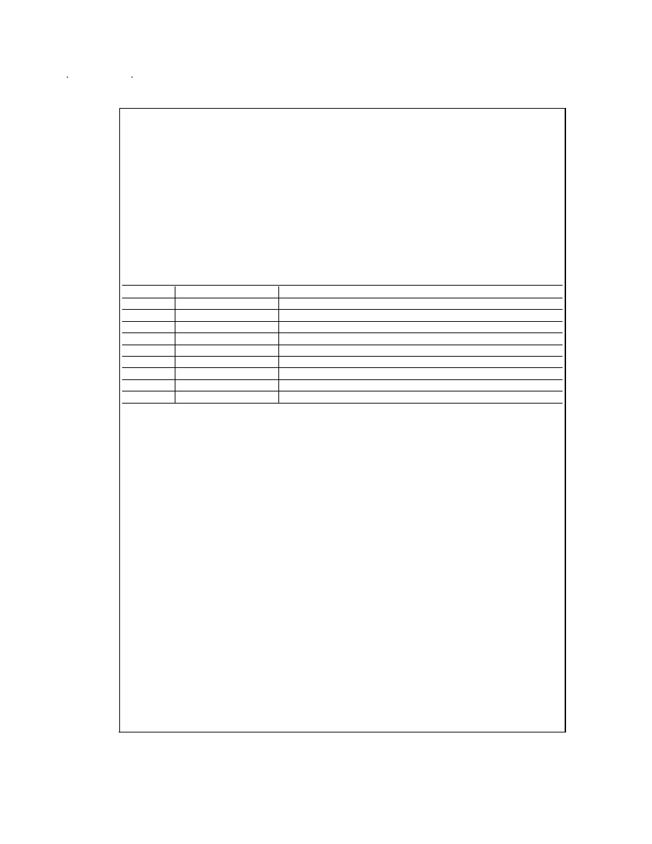
TABLE 1. Component Acceptable Value Range and Effected Parameters
Component
Acceptable Value Range
Parameters Effected
R1
100 k
≠1 M
Tolerated magnitude of invalid charger
R2
1 M
I
SUPPLY
vs. MOSFET turnoff delay
R3, R4
50
≠500
Current limit in extreme over voltage condition vs. IR drop of I
SUPPLY
R5
100 k
≠1 M
Current limit in pack ESD event vs. IR drop of I
ENABLE
R6
100 k
≠1 M
I
OL
vs. V
OH
of Full signal
C1
0.01 µF≠0.1 µF
Depends on frequency of noise loading the pack
C2
0.01 µF≠0.1 µF
Depends on impedance spectrum of Cells
C3
0.01 µF≠0.1 µF
Depends on MOSFET/Cell behavior during pack short circuit
C4
220 pF≠1 nF
Equally effective during pack short circuit
www.national.com
12
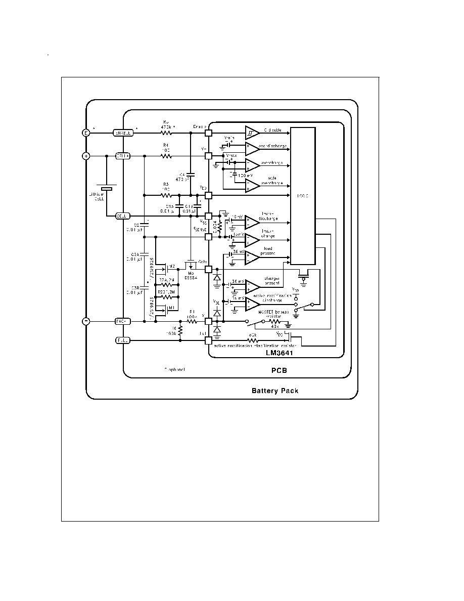
Application Circuit
The pack current flows through the series path of the cell, the
sense resistor and the power MOSFETs, M1 and M2. M3
isolates the IC against high compliance voltage chargers
when the power MOSFETs are OFF. The V- pin detects the
polarity of voltage across the power MOSFETs. R1 limits the
current into the V- pin when a charger is applied and the
MOSFETs are OFF. R3 and R4 limit the current into the IC in
the event of extreme charge current. They also prevent the
cell to be shorted when the V
DD
or V+ pin becomes shorted,
either internally or externally. R5 provides ESD protection of
the IC from the pack terminal "E". C1 bypasses transient Cell
currents so that the IC supply current is not interrupted. The
bypass of V
DD
is critical for stable operation, therefore it is
advised that 2 parallel bypass capacitors C1A and C1B be
used for redundancy. C2 is necessary to prevent the power
MOSFETs from oscillating when the pack is short circuited.
C3 suppresses possible oscillation of the MOSFETs during
pack short circuit. C3 can be duplicated for extra safety. The
same can be said for R2, which is used for proper turn OFF
of the MOSFETs during a fault condition. C4 isolates the En-
able pin from false reset signals during a pack short circuit
event. Series C2 and C3 also provide high frequency bypass
of the Cells which exhibit large impedance increase beyond
10≠100 kHz. R6 has to be added to pull up the Full pin. The
Enable section is optional. R5 and C4 are only needed if the
3rd terminal of the pack is used for the Enable function (see
Product Description, "Enable Pin" section). If not used, short
the Enable pin to the V
DD
pin.
DS012931-17
FIGURE 6. Application Circuit
www.national.com
13
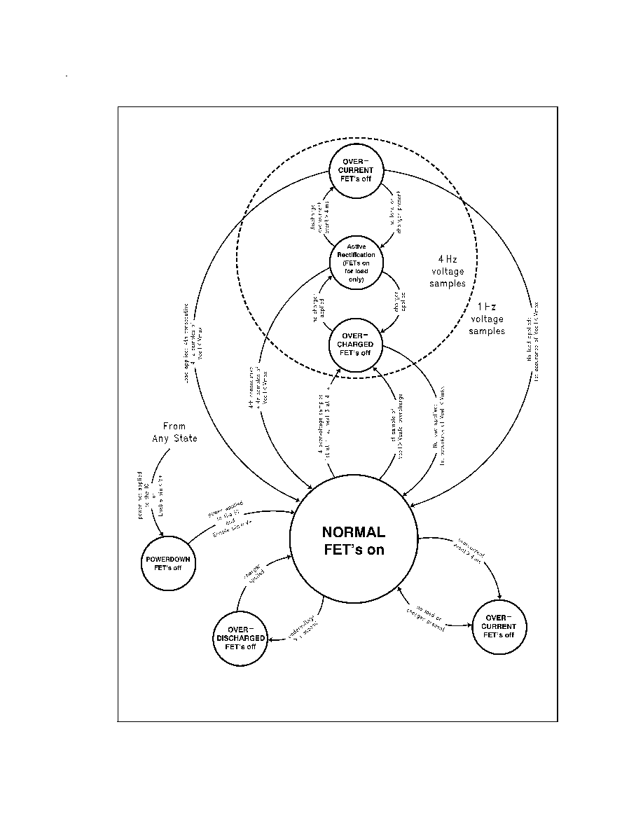
State Diagram
DS012931-19
FIGURE 7. State Diagram for LM3641 Operation
www.national.com
14

15
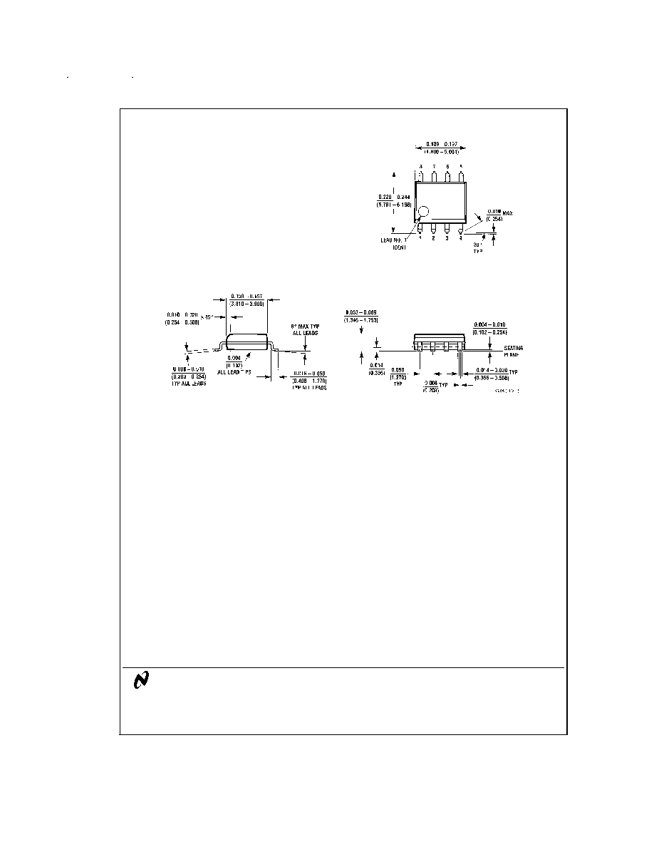
Physical Dimensions
inches (millimeters) unless otherwise noted
LIFE SUPPORT POLICY
NATIONAL'S PRODUCTS ARE NOT AUTHORIZED FOR USE AS CRITICAL COMPONENTS IN LIFE SUPPORT DE-
VICES OR SYSTEMS WITHOUT THE EXPRESS WRITTEN APPROVAL OF THE PRESIDENT OF NATIONAL SEMI-
CONDUCTOR CORPORATION. As used herein:
1. Life support devices or systems are devices or sys-
tems which, (a) are intended for surgical implant into
the body, or (b) support or sustain life, and whose fail-
ure to perform when properly used in accordance
with instructions for use provided in the labeling, can
be reasonably expected to result in a significant injury
to the user.
2. A critical component is any component of a life support
device or system whose failure to perform can be rea-
sonably expected to cause the failure of the life support
device or system, or to affect its safety or effectiveness.
National Semiconductor
Corporation
Americas
Tel: 1-800-272-9959
Fax: 1-800-737-7018
Email: support@nsc.com
www.national.com
National Semiconductor
Europe
Fax: +49 (0) 1 80-530 85 86
Email: europe.support@nsc.com
Deutsch Tel: +49 (0) 1 80-530 85 85
English
Tel: +49 (0) 1 80-532 78 32
FranÁais Tel: +49 (0) 1 80-532 93 58
Italiano
Tel: +49 (0) 1 80-534 16 80
National Semiconductor
Asia Pacific Customer
Response Group
Tel: 65-2544466
Fax: 65-2504466
Email: sea.support@nsc.com
National Semiconductor
Japan Ltd.
Tel: 81-3-5639-7560
Fax: 81-3-5639-7507
8-Lead SOIC (M08A)
Order Number LM3641M
NS Package Number M08A
This device is factory programmable. Contact your local NSC sales office for ordering information.
LM3641
Lithium-Ion
Battery
Pack
Protection
Circuit
National does not assume any responsibility for use of any circuitry described, no circuit patent licenses are implied and National reserves the right at any time without notice to change said circuitry and specifications.

This datasheet has been download from:
www.datasheetcatalog.com
Datasheets for electronics components.