LM3655
Charge Control and Protection IC for embedded single
cell Li-Ion/Polymer batteries
1.0 General Description
The LM3655 provides complete charge control, discharge
control and battery safety of a single Lithium-Ion cell. It
supports battery charging by using a variety of power supply
types including unregulated current-limited wall adapters,
regulated wall adapters and vehicle power adapters. Charge
current control is achieved using an external bipolar PNP
power transistor.
Furthermore, the LM3655 provides effective and compre-
hensive discharge control functionality. All operating load
current is supplied by the Li-Ion battery and passes through
this IC. This allows the battery power to disconnect due to
overload, short-circuit or low battery conditions. The IC also
offers extensive battery safety protection against over-
voltage and over-current. The internal safety circuit is
backed up by an identical circuit to provide safety redun-
dancy. The LM3655 requires minimal external components
and is packaged in a micro surface mount device for inte-
gration in a single cell battery pack.
2.0 Key Specifications
n
1% precision pin-selectable nominal 4.10V and 4.16V
termination voltages
n
Up to 1.2A full-rate charge current
n
Safety Shunt voltage 4.35V
n
800 mW power regulation of external PNP at 25�C
allows operation up to 30V (peak-to-peak) and 18V DC
3.0 Features
n
Input over-voltage protection for load and battery pack
n
Input over-current protection for load and battery pack
n
Reverse current protection
n
Reverse charger protection
n
Input short circuit protection that protects the cell from a
short on the charger-connector
n
Output overload current and short circuit protection
n
Complete charge control with pre-charging for depleted
batteries, full-rate and trickle charging.
n
Support for charging with regulated and non-regulated
wall adapters and vehicle power adapters.
n
Power regulation of the external Power PNP
n
Chemistry selection for Li-ion and Li-polymer
n
Complete linear Peak detector function for filtering ripple
on input power supply
n
Digital filtering of the cell voltage transients during
transmit pulses when LM3655 is used in a battery pack
for cell phones.
n
25-pin, 2.5 mm x 2.5 mm microSMD package for
mounting on four layered PCB inside the battery pack.
4.0 Applications
n
Cell phones and other portable applications which use
embedded Li-ion batteries
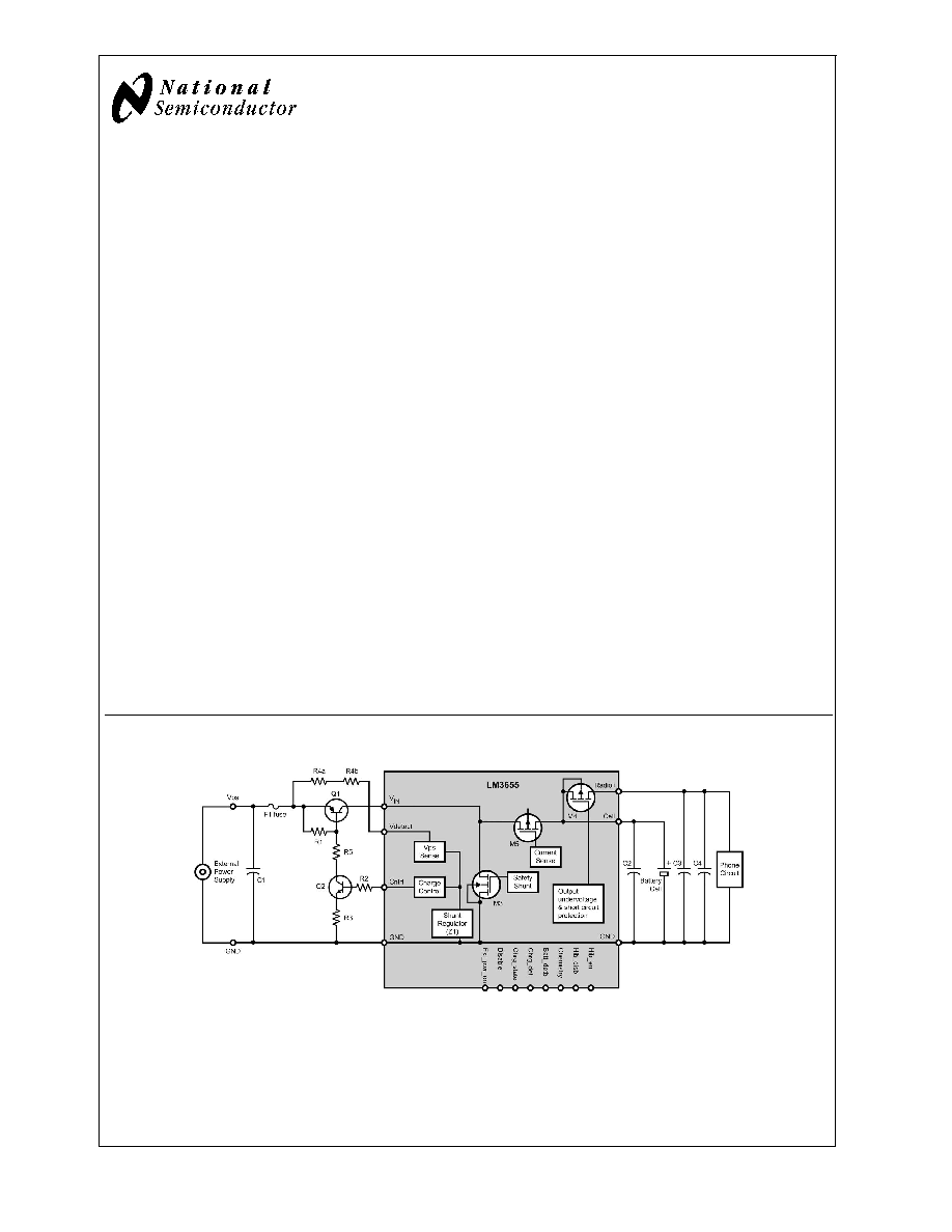
5.0 Typical Application Circuit
20111501
Because the LM3655 and associated external components provide safety protection for both the Li-Ion cell and the phone circuitry, appropriate precautions
must be taken in system design and layout to ensure proper operation.
November 2004
LM3655
Charge
Control
and
Protection
IC
for
embedded
single
cell
Li-Ion/Polymer
batteries
� 2004 National Semiconductor Corporation
DS201115
www.national.com

Table of Contents
1.0 General Description ..................................................................................................................................... 1
2.0 Key Specifications ........................................................................................................................................ 1
3.0 Features ....................................................................................................................................................... 1
4.0 Applications .................................................................................................................................................. 1
5.0 Typical Application Circuit ............................................................................................................................ 1
6.0 Connection Diagrams and Package Marking .............................................................................................. 3
7.0 LM3655 Pin Description ............................................................................................................................... 3
8.0 Ordering Information .................................................................................................................................... 4
9.0 Operation Description .................................................................................................................................. 4
10.0 Pin Functions ............................................................................................................................................. 4
10.1 V
IN
............................................................................................................................................................ 4
10.2 CELL ........................................................................................................................................................ 4
10.3 RADIO_B+ ............................................................................................................................................... 4
10.4 V
DETECT
................................................................................................................................................... 5
10.5 DISABLE ................................................................................................................................................. 5
10.6 CHEMISTRY ............................................................................................................................................ 5
10.7 HIB_EN .................................................................................................................................................... 5
10.8 HIS_DIS ................................................................................................................................................... 5
10.9 BATT_DETB ............................................................................................................................................ 5
10.10 CHRG_STATE ....................................................................................................................................... 5
10.11 CHRG_DET ........................................................................................................................................... 5
10.12 CNTRL ................................................................................................................................................... 5
10.13 EXT_PWR_ON ...................................................................................................................................... 6
11.0 Charge Control Functions .......................................................................................................................... 6
11.1 GENERAL OPERATION .......................................................................................................................... 6
11.2 EXTERNAL POWER SUPPLY DETECT ................................................................................................. 6
11.2.1 V
DETECT
Circuit ................................................................................................................................... 6
11.2.2 Debounce Function ............................................................................................................................ 7
11.2.3 Power Supply Test Pulses ................................................................................................................. 8
11.2.4 Low Cell Voltage Charging (Pre-Charging) ....................................................................................... 9
11.2.5 Full-Rate Charging ........................................................................................................................... 10
11.2.6 Trickle/Top-Off Mode ........................................................................................................................ 11
11.2.7 Peak Detector Function .................................................................................................................... 11
12.0 Discharge Control Functions .................................................................................................................... 12
12.1 GENERAL DESCRIPTION .................................................................................................................... 12
12.2 RADIO+ GENERATION ........................................................................................................................ 12
12.3 UNDER-VOLTAGE CUT-OFF ............................................................................................................... 13
12.4 POWER CUT OPERATION .................................................................................................................. 13
12.5 HIBERNATION MODE .......................................................................................................................... 13
13.0 Safety Functions ...................................................................................................................................... 13
13.1 INPUT OVER-VOLTAGE PROTECTION .............................................................................................. 13
13.1.1 Normal Operation (Q1 Control) ....................................................................................................... 13
13.1.2 Safety Shunt/Crowbar Operation ..................................................................................................... 14
13.1.3 Standby Shunt Mode ....................................................................................................................... 14
13.1.4 Thermal Crowbar Mode ................................................................................................................... 14
13.1.5 Fast Shunt Operation ...................................................................................................................... 14
13.1.6 Shunt Circuit Parametric Specifications .......................................................................................... 14
13.2 SCHOTTKY ELIMINATION MODE (CHARGER INPUT SHORT CIRCUIT/REVERSE CURRENT PRO-
TECTION) ...................................................................................................................................................... 15
13.3 REVERSE CHARGER PROTECTION .................................................................................................. 15
13.4 OUTPUT CURRENT OVERLOAD PROTECTION ("PTC" MODE) ...................................................... 15
13.5 OUTPUT SHORT CIRCUIT CURRENT PROTECTION ....................................................................... 15
14.0 Required External Components ............................................................................................................... 17
14.1 CHARGE PASS TRANSISTOR (Q1) .................................................................................................... 17
14.2 DRIVER TRANSISTOR AND BIAS RESISTORS (R2, R3 AND R5) .................................................... 17
14.3 EXTERNAL CHARGER SENSE RESISTOR (R4) ................................................................................ 17
14.4 CAPACITORS ........................................................................................................................................ 17
14.5 FUSE (F1) ............................................................................................................................................. 17
15.0 Electrical Characteristics .......................................................................................................................... 17
15.1 GENERAL SPECIFICATION AND ABSOLUTE MAXIMUM RATINGS
................................................ 17
15.2 PASS DEVICE AND POWER SUPPLY RATINGS ............................................................................... 18
15.3 IC PIN ELECTRICAL CHARACTERISTICS ......................................................................................... 18
LM3655
www.national.com
2
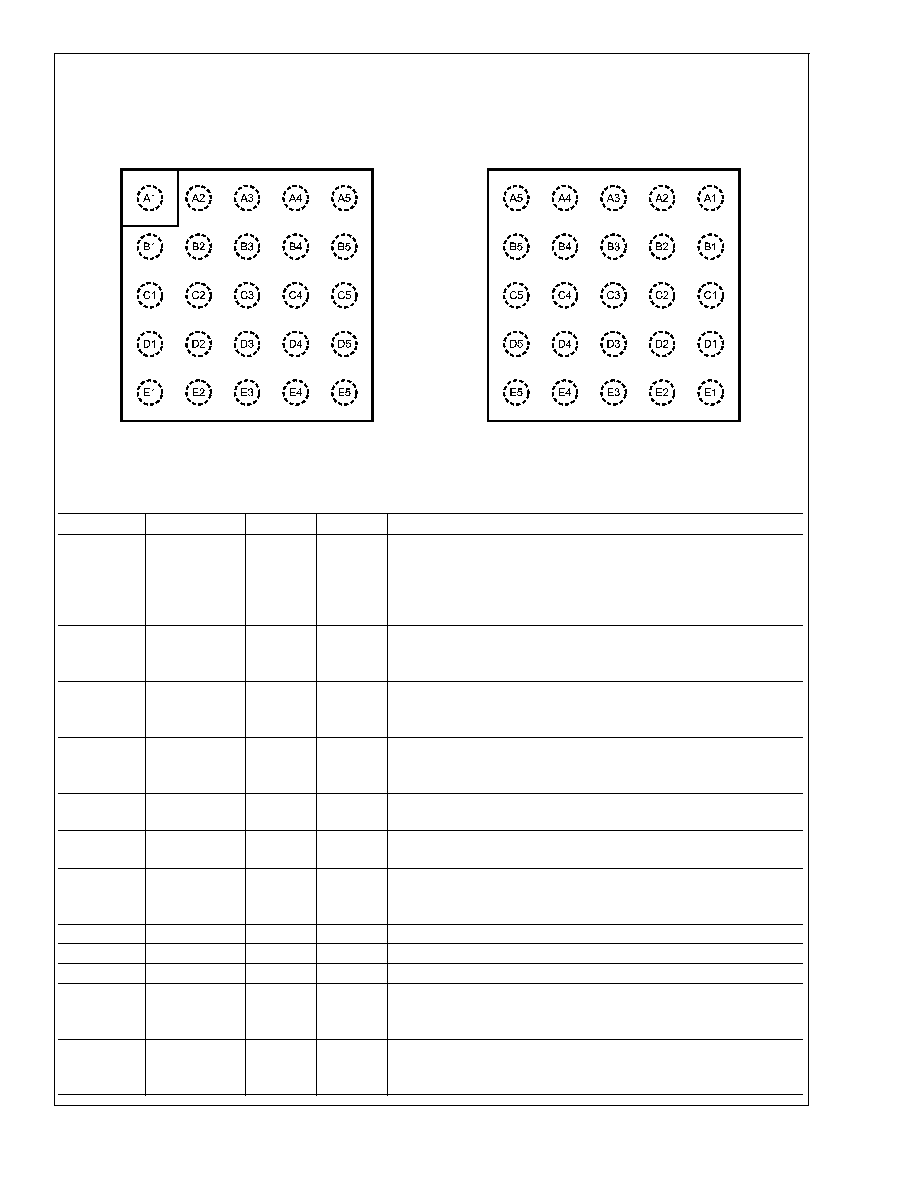
Table of Contents
(Continued)
16.0 Physical Dimensions ................................................................................................................................ 21
6.0 Connection Diagrams and Package Marking
20111502
MicroSMD Top View
See NS Package Number TLA25
20111503
MicroSMD Bottom View
7.0 LM3655 Pin Description
Pin #
Name
I/O
Type
Description
A1
CHEMISTRY
Input
Logic
A low input sets the constant voltage and termination voltage to the
lower V
TERML
. A high input sets the constant voltage to the higher
voltage level V
TERMH
. This pin has an internal 100 k
pull-down
resistor and can be controlled by a peripheral IC or can be tied directly
to B+ or GND.
A2
HIB_DISB
Input
Logic
This pin is internally pulled up to the CELL pin by a 100K resistor.
When this pin is momentarily pulsed low, Hibernate mode is exited,
which turns on M4.
A3
HIB_EN
Input
Analog
The IC is configured in hibernation mode, when this pin is pulled high
after a debounce period. Activating hibernation mode turns off the
internal M4 transistor.
A4
EXT_PWR_ON
Output
Logic
EXT_PWR_ON is a push-pull output. It is a logic 1 (Radio_B+ voltage
level) when the cell has reached the V
phone_on
level (nominally 3.0V)
while the charger is connected and the battery is present.
A5
CNTRL
Output
Analog
This output pin regulates the charger current by controlling the base
voltage of the external drive and pass transistors Q2 and Q1.
B1, C1, C2,
D1
RADIO
Output
Analog
This is the power supply terminal for the phone. ALL load current from
the cell must be sourced from this pin.
B2
NC
This pin must be left floating. It needs to be connected to a non
connected PCB pad for heat sinking. It cannot be connected to other
NC pins.
B3, C3, D3
CELL
I/O
Analog
These pins need to be connected to the cell's positive terminal.
B4, C4, D4
V
IN
Input
Analog
Input from the pass transistor Q1.
B5, C5, D5
GND
Ground
Ground pin for the circuit and CELL-
D2
NC
This pin must be left floating. It needs to be connected to a non
connected PCB pad for heat sinking. It cannot be connected to other
NC pins.
E1
DISABLE
Input
Logic
A logic high applied to this input disables the charging. A logic low
enables it. This pin has an internal 100 K
pull-down resistor and can
be left unconnected.
LM3655
www.national.com
3
7.0 LM3655 Pin Description
(Continued)
Pin #
Name
I/O
Type
Description
E2
BATT_DETB
Input
Logic
This pin is used to detect the presence of a battery. When the battery
is missing, the internal 100K resistor will pull up this pin to the voltage
on CELL. When the battery is present, this pin should be pulled low.
E3
CHRG_STATE
Output
Open
Drain
This pin is used to indicate the charge status. An external 30K pull-up
resistor needs to be connected between this pin and RADIO+ if output
on this pin is desired. A low output signifies that the IC is charging the
battery cell in full-rate mode. A high output indicates that trickle/top-off
charging is in process. The output is also high when the charger is
disabled (DIS pin tied high).
E4
CHRG_DETB
Output
Open
Drain
An external 30K pull-up resistor needs to be connected between this
pin and RADIO+ if output on this pin is desired. The CHRG_DETB
indicates whether an external power supply has been detected (output
= low) or not (output = high).
E5
VDET
Input
Analog
VDET provides the internal control with a signal that is proportional to
the external voltage level and also provides power to the internal
control circuitry.
8.0 Ordering Information
Order Number
Packaging Type
NSC Package
Marking (*)
Supplied As
LM3655TL
25-bump Wafer Level
Chip Scale
(micro SMD)
XY TT S50
250 units, Tape-and-Reel
LM3655TLX
XY TT S50
3000 units, Tape-and-Reel
(*) XY - denotes the date code marking (2 digits) in production
(*) TT - refers to die/lot tracking for production
(*) S - product line designator
Package markings may change over the course of production
9.0 Operation Description
Refer to Typical Application Circuit for external and internal component reference designators such as Q1, M5, etc.
10.0 Pin Functions
10.1 V
IN
V
IN
is the input pin for the charging current from the external power source to the battery/cell. When the phone is operating from
an external supply, cell phone operating current also passes through this pin. Total input current into the V
IN
pin is internally
sensed by monitoring the voltage drop across the series sensing FET M5.
V
IN
is derived from the output (collector) of Q1, and not directly connected to the external source. If the external power supply
(VPS) potential exceeds a maximum safe limit, Q1 will be controlled to protect the cell and phone circuits from over-voltage. Q1
provides the primary over-voltage protection mechanism for the phone circuits and the cell.
10.2 CELL
CELL is connected directly to the battery/cell positive terminal. Under normal operation of the phone, it serves as the main power
supply pin for the LM3655.
When the phone is drawing current from the battery, current will flow into this pin and out through the internal FET M4 to supply
the phone's operating rail (RADIO_B+). When connected to an external supply to charge the battery, current will flow through M5
and out of this pin into the cell. If the phone is being operated while connected to an external power supply, the phone's operating
current (current out of the RADIO_B+ pin) will be the sum of the currents into the CELL and V
IN
pins.
10.3 RADIO_B+
All power for the phone's operation (other than battery charging) is derived from this pin. The phone's operating current flows
through M4, which is controlled and monitored to prevent overload or short-circuit currents, and disabled during cell under-voltage
conditions.
LM3655
www.national.com
4

10.0 Pin Functions
(Continued)
10.4 V
DETECT
This pin is coupled to the external power supply through a series resistance (R4). It is used to determine when an external source
(charger) is connected, which in turn initiates the device's charge control logic. The CHRG_DETB output is set based on input to
this pin.
10.5 DISABLE
The phone can stop the charge current through use of the DISABLE logic input pin of the IC. Asserting a logic high on the
DISABLE Pin of the IC will force the control pin (CNTRL) to turn off the external Drive (Q2) and Pass (Q1) transistors so there
is no charge current to the cell. The DISABLE input can be driven high by the phone's logic at any time to interrupt the charge
current. Use of the DISABLE pin during charging can allow the phone to measure the cell's true voltage by peripheral circuitry
(without the presence of charge current input) if desired.
Additionally, a high-to-low transition on the DISABLE pin (thus re-enabling the charger operation), will reset the charge control
state machine.
10.6 CHEMISTRY
The CHEMISTRY pin provides a logic input to the IC that determines the termination threshold for Li-ion cell charging. A logic low
applied to this pin selects the lower charging threshold or termination voltage (V
TERML
), a logic high selects the higher charging
threshold (V
TERMH
).
Because different cell types may require slightly different charge termination thresholds, the LM3655 supports a pin-
programmable selection between two different settings. The lower threshold is nominally 4.10V, and the higher threshold is
nominally 4.16V.
10.7 HIB_EN
This pin provides a logic input to the IC that when held high during a debounce period of 32 mS, M4 will be latched open even
if the cell voltage is above V
CHARGE_LOW
. This pin has a 10K pull-down resistor internal to the IC so that the IC will default on.
10.8 HIS_DIS
This pin provides a logic input to the IC that when held low momentarily, the latch holding M4 open is cleared allowing it to be
closed when the cell voltage is above V
CHARGE_LOW
. This pin has a 100K pullup resistor to the CELL pin internal to the IC.
10.9 BATT_DETB
BATT_DETB indicates to the LM3655 IC that a cell is present in the system. This pin provides a logic input to the IC that when
held low, the IC will be able to detect the presence of a charger. There is a 100K pull-up resistor internal to the IC on this pin, which
is supplied from the charger (not from the cell).
A series 10K resistor is to be used between this pin and the removable battery to protect the IC against ESD.
10.10 CHRG_STATE
CHRG_STATE is an open-drain logic output to the phone, and can be used to provide a simple battery-metering indication during
charge mode. During charge mode, with current flowing into the cell, the Li-ion cell voltage cannot be used for an accurate
indication of state of charge. If a battery is at a relatively low state of charge, it will remain in the "full-rate" charge mode for some
period of time when connected to the external power supply. When the cell reaches a higher state of charge, the charge control
switches to the trickle/top-off mode. Thus, this signal is logic low during full-rate charge mode and high during the trickle/top-off
mode. The exact percentage of "full" at this crossover point will vary depending on many conditions, primarily full-rate charge
current level, but is expected to be
>
60% for typical use with a mid-rate charger.
This information can be used to provide a simple "charging" or "ready" indication by the system for the battery status meter during
charge. If combined with a timer, or other means of interaction by the system (such as periodic control of the DISABLE pin
combined with cell voltage measurements during periods of no current flow) a more complete metering method may be
implemented if desired.
10.11 CHRG_DET
This is an open-drain output to the phone's power management IC that indicates the connection of an external power supply.
Typical application uses a 30K pull-up resistor to RADIO_B+. When a charger is detected, this output is pulled LOW by the
internal logic of the LM3655. This signal may be pulled up to a low-voltage logic rail such as 2.75V or 1.8V regulated voltage. It
is assumed that the voltage used to pull-up is no higher than the cell voltage.
10.12 CNTRL
This is an analog output to control Q2, the NPN drive transistor. The CNTRL output is adjusted to deliver the appropriate level of
current required by the charge algorithm for full-rate or trickle/top-off charging. During full-rate charging, CNTRL is set such that
Q1 will be saturated. During trickle/top-off mode, CNTRL will be set in order to maintain the appropriate cell clamp voltage (4.10V
or 4.16V as desired). Furthermore, if the power-monitoring circuit determines that excess power is being dissipated in, the CNTRL
signal will be further reduced to limit current flowing through Q1. This ensures that the Q1 pass device remains within safe power
dissipation limits.
LM3655
www.national.com
5