 | ÐлекÑÑоннÑй компоненÑ: LM3658SDX | СкаÑаÑÑ:  PDF PDF  ZIP ZIP |
Äîêóìåíòàöèÿ è îïèñàíèÿ www.docs.chipfind.ru
LM3658
Dual Source USB/AC Li Chemistry Charger IC for
Portable Applications
General Description
The LM3658 is a single chip charger IC designed for hand-
held applications. It can safely charge and maintain a single
cell Li-Ion/Polymer battery operating from an AC wall
adapter or USB power source. Input power source selection
of USB/AC is automatic. With both power sources present,
the AC power source has priority. Charge current is pro-
grammed through an external resistor when operating from
an AC wall adapter allowing charge currents from 50 mA to
1000 mA. When the battery is charged using USB power,
charge currents of 100 mA or 500 mA are pin-selectable. The
termination voltage is controlled to within
±
0.35% of 4.2V.
The LM3658 requires few external components and inte-
grates internal power FETs, reverse current protection and
current sensing. The internal power FETs are thermally regu-
lated to obtain the most efficient charging rate for a given
ambient temperature.
The LM3658 operates in five modes: pre-qualification mode,
constant-current mode, constant-voltage mode, top-off
mode and maintenance mode. Optimal battery management
is obtained through thermal regulation, battery temperature
measurement and multiple safety timers. The LM3658 pro-
vides two open-drain outputs for LED status indication or
connection to GPIOs.
Features
n
Integrated power FETs with thermal regulation
n
Charges from either an AC wall adapter or USB power
source with automatic source selection
n
50 mA to 1000 mA charge currents using AC wall
adapter
n
Pin-selectable USB charge currents of 100 mA or
500 mA
n
Continuous battery temperature monitoring
n
Built-in multiple safety timers
n
Charge status indication
n
Continuous over-current and temperature protection
n
Near-depleted battery pre-conditioning
n
Sleep mode with ultra low quiescent current
n
On-board Kelvin-sensing achieves
±
0.35% termination
accuracy
n
Maintenance mode with automatic recharge
n
Thermally enhanced 3 mm x 3 mm LLP package
Applications
n
Smartphones
n
Digital still cameras
n
PDAs
n
Hard Drive and flash-based MP3 players
n
USB-powered devices
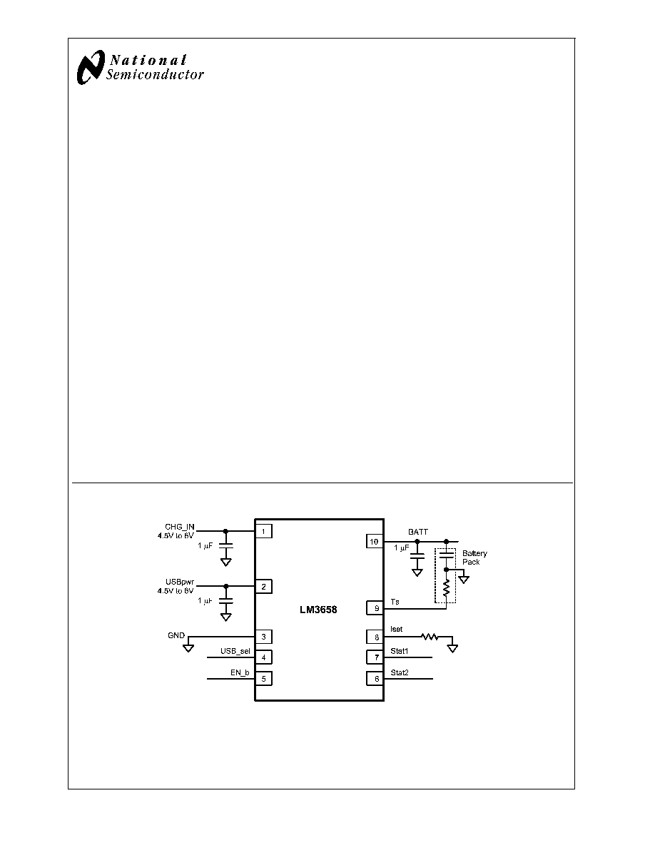
Typical Application
20128201
May 2005
LM3658
Dual
Source
USB/AC
Li
Chemistry
Charger
IC
for
Portable
Applications
© 2005 National Semiconductor Corporation
DS201282
www.national.com
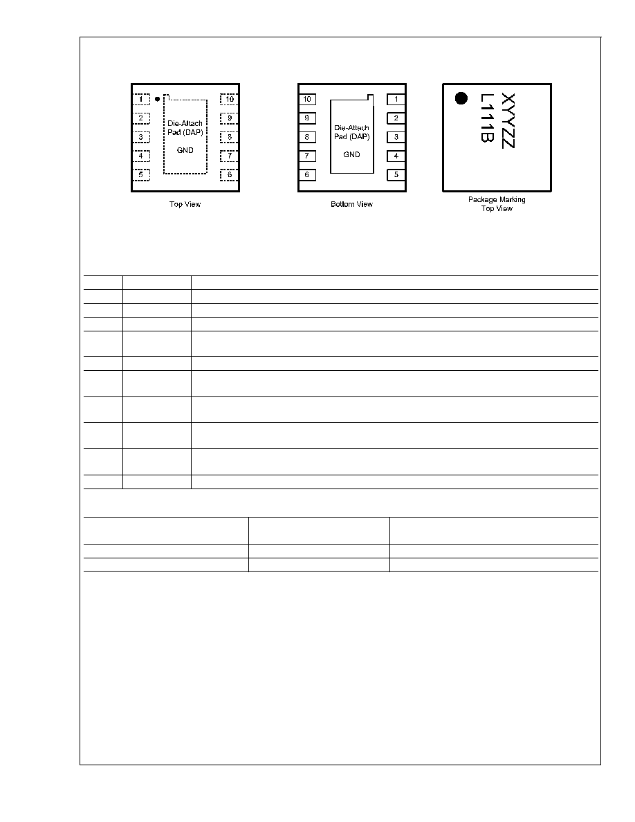
Connection Diagram and Package Mark Information
LLP10 Package Drawing
20128202
Note: The actual physical placement of the package marking will vary from part to part. The package marking "X" is the manufacturing plant code. "YY" is a
2-digit date code, and "ZZ" for die traceability. These codes will vary considerably. "L111B" identifies the device (part number, option, etc.).
TABLE 1. LM3658 Pin Description
Pin #
Name
Description
1
CHG_IN
AC wall adapter input pin.
2
USBpwr
USB power input pin.
3
GND
Power and signal ground pin.
4
USB_sel
Pulling this pin low limits the USB charge current to 100 mA. Pulling this pin high limits the USB
charge current to 500 mA.
5
EN_b
Pulling this pin low enables the charger. Pulling this pin high disables the charger.
6
STAT2
Active low open-drain output. Indicates charger status. This pin is capable of driving an LED as well
as GPIOs. See Operation Description section for more detail.
7
STAT1
Active low open-drain output. Indicates charger status. This pin is capable of driving an LED as well
as GPIO. See Operation Description section for more detail.
8
I
SET
A resistor is connected between this pin and GND. The resistor value determines the full-rate charge
current when using the AC source.
9
T
S
Battery temperature sense pin. This pin must be connected to battery pack's temperature sense
output pin. See Operation Description section for more detail.
10
BATT
Positive battery terminal connection.
TABLE 2. Ordering Information
Order Number
Package
Marking
Supplied As
LM3658SD
L111B
1000 units, Tape-and-Reel
LM3658SDX
L111B
4500 units, Tape-and-Reel
For more information on the various options, please refer to Operation Description section.
LM3658
www.national.com
2
Absolute Maximum Ratings
(Notes 1,
2)
If Military/Aerospace specified devices are required,
please contact the National Semiconductor Sales Office/
Distributors for availability and specifications.
CHG_IN, USBpwr (V
CC
)
-0.3V to +6.5V
All other pins except GND
-0.3V to CHG_IN or USBpwr
Power Dissipation (Note 3)
Internally Limited
Junction Temperature (T
J-MAX)
+150°C
Storage Temperature Range
-65°C to +150°C
ESD Rating (Note 4)
Human Body Model:
Machine Model:
2.0 kV
200V
Operating Ratings
(Notes 1, 2)
Input Voltage Range for CHG_IN
4.5V to 6.0V
Input Voltage Range for USB_pwr
4.35V to 6.0V
Recommended Load Current
0 to 1000 mA
Power Dissipation(Note 3)
Internally Limited
Junction Temperature (T
J
) Range
-40°C to +125°C
Ambient Temperature (T
A
) Range
-40°C to +85°C
Thermal Properties
JA
, Junction-to-Ambient Thermal
54°C/W
Resistance (Note 5)
Electrical Characteristics
Unless otherwise noted, V
CC
(V
CHG_IN
and/or V
USBpwr
) = 5V, V
BATT
= 3.5V.
C
CHG_IN
= 1 µF, C
USBpwr
= 1 µF, C
BATT
= 1 µF. Typical values and limits appearing in normal type apply for T
J
= 25°C. Limits
appearing in boldface type apply over T
J
= 0°C to +85°C. (Notes 2, 6, 7)
Symbol
Parameter
Conditions
Typ
Limit
Units
Min
Max
CHARGER
V
CHG_IN
AC Wall Adapter
Input Voltage Range
4.5
6.0
V
V
USBpwr
USB Input Voltage
Range
4.35
6.0
V
I
CC_PD
Quiescent Current in
Power Down Mode
V
BATT
>
V
CC
V
OK_CHG
1
5
µA
I
CC_STBY
Quiescent Current in
Standby Mode
V
BATT
<
V
CC
- V
OK_CHG
V
CC
>
V
POR
EN_b = High
400
600
µA
I
BATT_PD
Battery Leakage
Current in Power
Down Mode
V
BATT
>
V
CC
+ V
OK_CHG
0.01
2.0
µA
I
BATT_MAINT
Battery Leakage
Current in
Maintenance Mode
STAT1 = off, STAT2 = on, adapter or USB
connected, V
BATT
= 4.2V
7
15
µA
V
OK_CHG
CHG_IN or USBpwr
OK Trip-Point
V
CC
V
BATT
(Rising)
V
CC
V
BATT
(Falling)
200
50
mV
V
POR
V
CC
POR Trip-Point
V
CC
(Rising)
V
BATT
<
V
CC
V
OK_CHG
V
FULL_RATE
<
V
BATT
<
V
TERM
3.0
V
V
TERM
Battery Charge
Termination Voltage
I
CHG
= 10% of its value when V
BATT
= 3.5V
4.2
V
Battery Charge
Termination Voltage
Tolerance
T
A
= 25°C
-0.35
+0.35
%
T
A
= 0°C to 85°C
-1.5
+1.5
V
CHG_DO
CHG_IN Drop-Out
Voltage
V
BATT
= V
TERM
, I
CHG
= 1A
V
CC
>
V
BATT
+ V
CHG_DO_MAX
500
mV
V
USB_DO
USBpwr Drop-Out
Voltage
V
BATT
= V
TERM
, USB_sel = high
V
CC
>
V
BATT
+ V
USB_DO_MAX
250
mV
I
CHG
CHG_IN Full-Rate
Charge Current
Range (see full-rate
charge mode
description)
6V
V
CC
4.5V
V
BATT
<
V
CC
V
OK_CHG
V
FULL_RATE
<
V
BATT
<
V
TERM
I
CHG
= K
ISET
/R
ISET
50
1000
mA
LM3658
www.national.com
3

Electrical Characteristics
Unless otherwise noted, V
CC
(V
CHG_IN
and/or V
USBpwr
) = 5V, V
BATT
= 3.5V.
C
CHG_IN
= 1 µF, C
USBpwr
= 1 µF, C
BATT
= 1 µF. Typical values and limits appearing in normal type apply for T
J
= 25°C. Limits
appearing in boldface type apply over T
J
= 0°C to +85°C. (Notes 2, 6, 7) (Continued)
Symbol
Parameter
Conditions
Typ
Limit
Units
Min
Max
CHARGER
I
CHG
CHG_IN Full Rate
Charge Current
R
ISET
= 10k
245
220
270
mA
R
ISET
= 5 k
500
465
535
R
ISET
= 3.3k
760
700
820
K
ISET
Charge Current Set
Coefficient
I
CHG
= K
ISET
/R
ISET
(see full-rate charge
mode description)
6V
V
CC
4.5V
V
BATT
<
V
CC
V
OK_CHG
V
FULL_RATE
<
V
BATT
<
V
TERM
2500
A
V
ISET
Charge Current Set
Voltage
6V
V
CC
4.5V
V
BATT
<
V
CC
V
OK_CHG
V
FULL_RATE
<
V
BATT
<
V
TERM
2.5
V
I
USB_L
USB Full-Rate
Charge Low Current
90
80
100
mA
I
USB_H
USB Full-Rate
Charge High Current
450
400
500
mA
I
PREQUAL
Pre-Qualification
Current
V
BATT
= 2V, for both AC adapter and USB
45
35
55
mA
V
FULL_RATE
Full-Rate
Qualification
Threshold
V
BATT
rising, transition from pre-qualification to
full-rate charging
3.0
2.9
3.1
V
Full Rate Hysteresis
V
BATT
falling
60
50
70
mV
I
EOC
End-of-Charge
Current, Percent from
Full-Range Current
6V
V
CC
4.5V
V
BATT
<
V
CC
V
OK_CHG
V
FULL_RATE
<
V
BATT
<
V
TERM
9
7
11
%
I
TOPOFF
Minimum Top-Off
Charge Current
6V
V
CC
4.5V
V
BATT
<
V
CC
V
OK_CHG
V
BATT
= V
TERM
2.5
1.25
3.75
%
V
RESTART
Restart Threshold
Voltage
V
BATT
falling, transition from EOC to
pre-qualification mode
4.0
3.94
4.07
V
V
TL
Battery Temperature
Sense Comparator
Low-Voltage
Threshold
0.49
0.46
0.52
V
V
TH
Battery Temperature
Sense Comparator
High-Voltage
Threshold
2.49
2.44
2.54
V
I
TSENSE
Battery Temperature
Sense Current
100
94
106
µA
T
REG
Regulated Junction
Temperature
120
°C
T
SD
Thermal Shutdown
Temperature
165
°C
DETECTION AND TIMING
T
POK
Power OK Deglitch
Time
V
BATT
<
V
CC
V
OK_CHG
60
40
100
ms
T
PREQUAL
Pre-Qualification
Timer
30
27
33
mins
LM3658
www.national.com
4
Electrical Characteristics
Unless otherwise noted, V
CC
(V
CHG_IN
and/or V
USBpwr
) = 5V, V
BATT
= 3.5V.
C
CHG_IN
= 1 µF, C
USBpwr
= 1 µF, C
BATT
= 1 µF. Typical values and limits appearing in normal type apply for T
J
= 25°C. Limits
appearing in boldface type apply over T
J
= 0°C to +85°C. (Notes 2, 6, 7) (Continued)
Symbol
Parameter
Conditions
Typ
Limit
Units
Min
Max
DETECTION AND TIMING
T
PQ_FULL
Deglitch Time for
Pre-Qualification to
Full-Rate Charge
Transition
300
270
330
ms
T
FULL_PQ
Deglitch Time for
Full-Rate to
Pre-Qualification
Transition
300
270
330
ms
T
CHG
Charge Timer
300
270
330
min
T
EOC
Deglitch Time for
End-of-Charge
Transition
300
270
330
ms
T
BATTEMP
Deglitch Time for
Battery Temperature
Fault
40
20
80
ms
T
DGL
Deglitch Time for
EN_b and USB_sel
Pins
40
20
80
ms
T
ITOPOFF
Deglitch Time for
I
TOPOFF
300
270
330
ms
T
TOPOFF
Top-Off Charging
Timer
30
27
33
min
I/O
V
IL
Low-Level Input
Voltage
EN_b
0
0.7
V
USB_sel
1.5
V
IH
High-Level Input
Voltage
EN_b
1.4
V
USB_sel
2.5
I
OL
Low-Level Output
Current
STAT1, STAT2, output voltage = 0.25V
25
10
mA
I
OH
High-Level Output
Current
STAT1, STAT2, output voltage = 6.0V
0.01
1
µA
Note 1: Absolute Maximum Ratings indicate limits beyond which damage to the component may occur. Operating Ratings are conditions under which operation of
the device is guaranteed. Operating Ratings do not imply guaranteed performance limits. For guaranteed performance limits and associated test conditions, see the
Electrical Characteristics tables.
Note 2: All voltages are with respect to the potential at the GND pin.
Note 3: The LM3658 has built-in thermal regulation to regulate the die temperature to 120
o
C. See Operation Description section for more detail.
Note 4: The Human body model is a 100 pF capacitor discharged through a 1.5 k
resistor into each pin. The machine model is a 200 pF capacitor discharged
directly into each pin. MIL-STD-883 3015.7
Note 5: Junction-to-ambient thermal resistance is highly application and board-layout dependent. In applications where high maximum power dissipation exists,
special care must be paid to thermal dissipation issues in board design. Please refer to application note AN1187 for more detail.
Note 6: Min and Max limits are guaranteed by design, test, or statistical analysis. Typical numbers are not guaranteed, but do represent the most likely norm.
Note 7: LM3658 is not intended as a Li-Ion battery protection device; battery used in this application should have an adequate internal protection.
LM3658
www.national.com
5
Document Outline