 | –≠–ª–µ–∫—Ç—Ä–æ–Ω–Ω—ã–π –∫–æ–º–ø–æ–Ω–µ–Ω—Ç: LM368H-10 | –°–∫–∞—á–∞—Ç—å:  PDF PDF  ZIP ZIP |
TL H 5522
LM368-50
and
LM368-10
Precision
Voltage
References
January 1995
LM368-5 0 and LM368-10 Precision Voltage References
General Description
The LM368 is a precision monolithic temperature-compen-
sated voltage reference The LM368 makes use of thin-film
technology enhanced by the discrete laser trimming of re-
sistors
to
achieve
excellent
Temperature
coefficient
(Tempco) of V
OUT
(as low as 5ppm C) along with tight
initial tolerance (as low as 0 02%) The trim scheme is such
that individual resistors are cut open rather than being
trimmed (partially cut) to avoid resistor drift caused by elec-
tromigration in the trimmed area The LM368 also provides
excellent stability vs changes in input voltage and output
current (both sourcing and sinking) This device is available
in output voltage options of 5 0V and 10 0V and will operate
in both series or shunt mode Also see the LM368-2 5 data
sheet for a 2 5V output The devices are short circuit proof
when sourcing current A trim pin is made available for fine
trimming of V
OUT
or for obtaining intermediate values with-
out greatly affecting the Tempco of the device
Features
Y
300 mA operating current
Y
Low output impedance
Y
Excellent line regulation ( 0001% V typical)
Y
Single-supply operation
Y
Externally trimmable
Y
Low temperature coefficient
Y
Operates in series or shunt mode
Y
10 0V or 5 0V
Y
Excellent initial accuracy (0 02% typical)
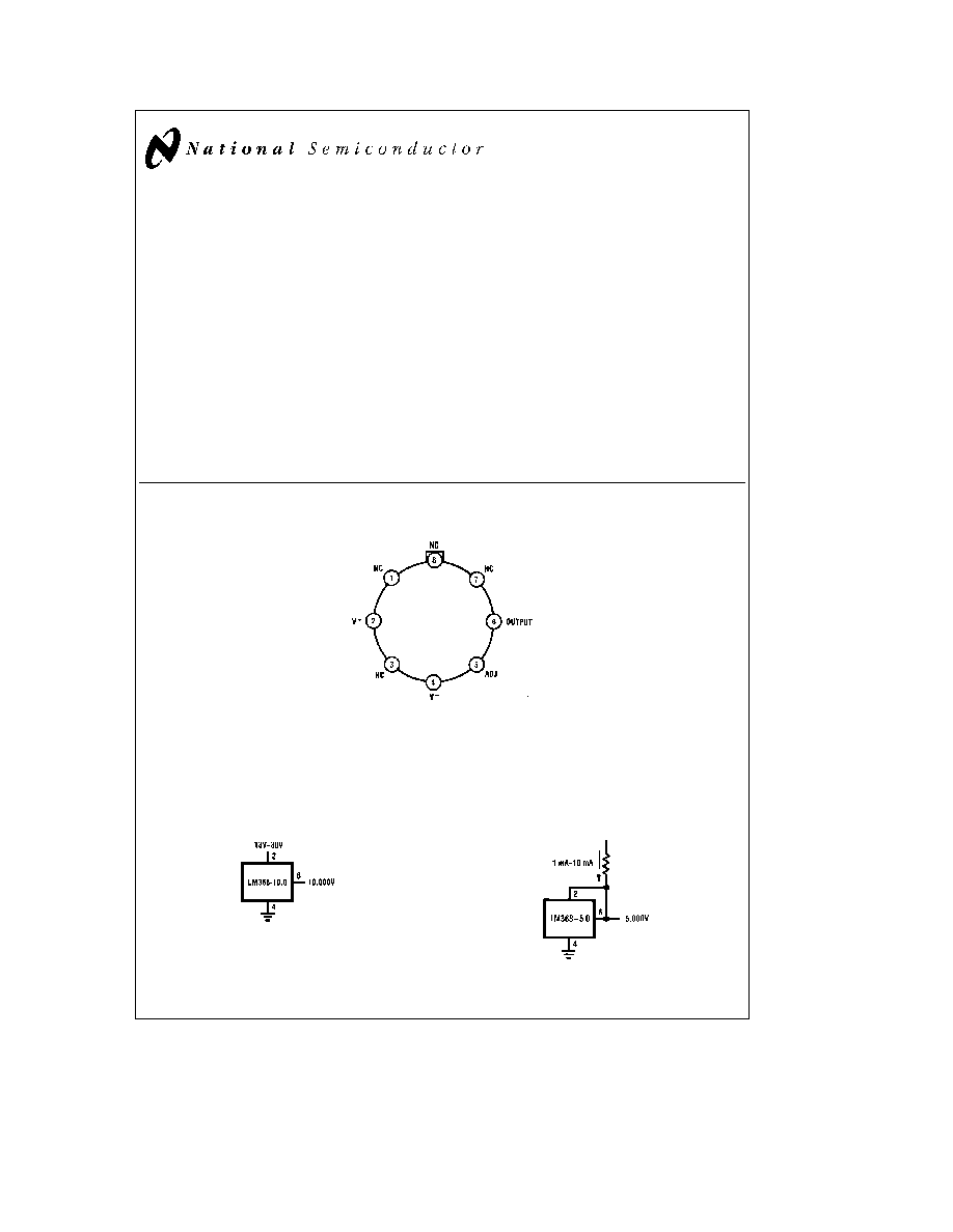
Connection Diagram
Metal Can Package
TL H 5522 ≠ 1
Top View
case connected to V
b
Order Number LM368YH-10
LM368YH-5 0 LM368H-10 LM368H-5 0
See NS Package Number H08C
Typical Applications
Series Regulator
TL H 5522 ≠ 2
Shunt Regulator
TL H 5522 ≠ 3
C1995 National Semiconductor Corporation
RRD-B30M115 Printed in U S A
Absolute Maximum Ratings
(Note 8)
Input Voltage (Series Mode)
35V
Reverse Current (Shunt Mode)
50 mA
Power Dissipation
600 mW
Storage Temperature Range
b
60 C to
a
150 C
Operating Temperature Range
LM368
0 C to
a
70 C
Soldering Information
TO-5 (H) Package 10 sec
a
300 C
See AN-450 ``Surface Mounting Methods and Their Effect
on Product Reliability'' (Appendix D) for other methods of
soldering surface mount devices
Electrical Characteristics
(Note 1)
LM368
Tested
Design
Units
Parameter
Conditions
Typical
Limit
Limit
(Max unless
(Note 2)
(Note 3)
noted)
V
OUT
Error
g
0 02
g
0 1
%
Line Regulation
(V
OUT
a
3V)
s
V
IN
s
30V
g
0 0001
g
0 0005
% V
Load Regulation
0 mA
s
I
SOURCE
s
10 mA
g
0 0003
g
0 001
% mA
(Note 4)
b
10 mA
s
I
SINK
s
0 mA
g
0 003
g
0 008
% mA
Thermal Regulation
T
e
20 mS (Note 5)
g
0 005
g
0 01
% 100 mW
Quiescent Current
250
350
m
A
Change of Quiescent Current vs V
IN
(V
OUT
a
3V)
s
V
IN
s
30V
3
5
m
A V
Temperature Coefficient
of V
OUT
(see graph) LM368Y
0 C
s
T
A
s
70 C
g
11
g
20
ppm C
(Note 6)
LM368
0 C
s
T
A
s
70 C
g
15
g
30
ppm C
Short Circuit Current
V
OUT
e
0
30
70
100
mA
Noise
10 0V 0 1 - 10Hz
30
uVp-p
100Hz - 10 kHz
1100
nV
0
Hz
6 2V 0 1 - 10Hz
20
uVp-p
100Hz - 10 kHz
700
nV
0
Hz
5 0V 0 1 - 10Hz
16
uVp-p
100Hz - 10 kHz
575
nV
0
Hz
V
OUT
Adjust Range 10 000V
0V
s
V
PIN5
s
V
OUT
4 5-17 0
6 0-15 5
V min
5 000V
4 4-7 0
4 5-6 0
V min
Note 1
Unless otherwise noted these specifications apply T
A
e
25 C V
IN
e
15V I
LOAD
e
0 0
s
C
L
s
200 pF Circuit is operating in Series Mode Or circuit is
operating in Shunt Mode V
IN
e a
15V or V
IN
e
V
OUT
TA
e a
25 C I
LOAD
e b
1 0 mA 0
s
C
L
s
200 pF
Note 2
Tested Limits are guaranteed and 100% tested in production
Note 3
Design Limits are guaranteed (but not 100% production tested) over the indicated temperature and supply voltage ranges These limits are not used to
calculate outgoing quality levels
Note 4
The LM368 has a Class B output and will exhibit transients at the crossover point This point occurs when the device is asked to sink approximately
120 mA In some applications it may be advantageous to preload the output to either V
IN
or Ground to avoid this crossover point
Note 5
Thermal Regulation is defined as the change in the output Voltage at a time T after a step change in power dissipation of 100 mW
Note 6
Temperature Coefficient of V
OUT
is defined as the worst case delta-V
OUT
measured at Specified Temperatures divided by the total span of the Specified
Temperature Range (See graphs) There is no guarantee that the Specified Temperatures are exactly at the minimum or maximum deviation
Note 7
In metal can (H) i
J≠C
is 75 C W and i
J≠A
is 150 C W
Note 8
Absolute Maximum Ratings indicate limits beyond which damage to the device may occur DC and AC electrical specifications do not apply when operating
the device beyond its Rated Operating Conditions (see Note 1 and Conditions)
2
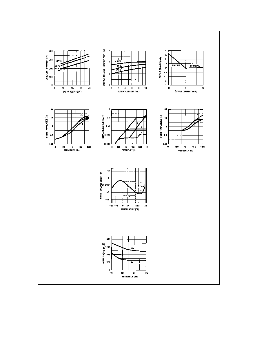
Typical Performance Characteristics
(Note 1)
Voltage and Temperature
Quiescent Current vs Input
(Series Mode Sourcing Current)
Dropout Voltage vs Output Current
Output Current
Output Change vs
(Sourcing Current)
Output Impedance vs Frequency
Ripple Rejection vs Frequency
(Sinking Current)
Output Impedance vs Frequency
LM368-10 (Curve A)
Temperature Coefficient
TL H 5522 ≠ 4
Typical Temperature Coefficient Calculations
LM368-10 (see Curve A)
T C
e
7 7 mV (70
c
10V)
e
11
c
10E-6
e
11ppm C
Output Noise vs Frequency
TL H 5522 ≠ 5
(1) LM368 alone
(2) with 0 01 mf Mylar Trim to Gnd
(3) with 10X in series with 10 mf V
OUT
to Gnd
(4) with Both
3
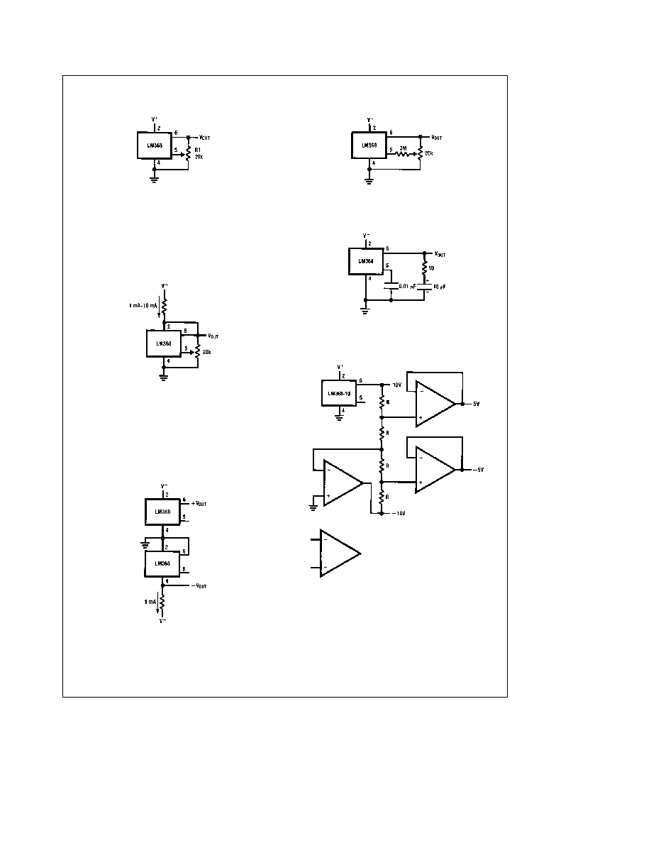
Typical Applications
Wide Range Trimmable Regulator
TL H 5522 ≠ 7
Adjustable Zener
TL H 5522 ≠ 9
g
Reference
TL H 5522 ≠ 11
Narrow Range Trimmable Regulator (
g
1% min )
TL H 5522 ≠ 8
Improved Noise Performance
TL H 5522 ≠ 10
g
10V
g
5V References
e
LF444A or
LF412A
TL H 5522 ≠ 12
R
e
Thin Film Resistor Network
g
0 05% Matching and 5ppm Tracking
(Beckman 694-3-R-10K-A)
(Caddock T-914-10K-100-05)
or similar
4
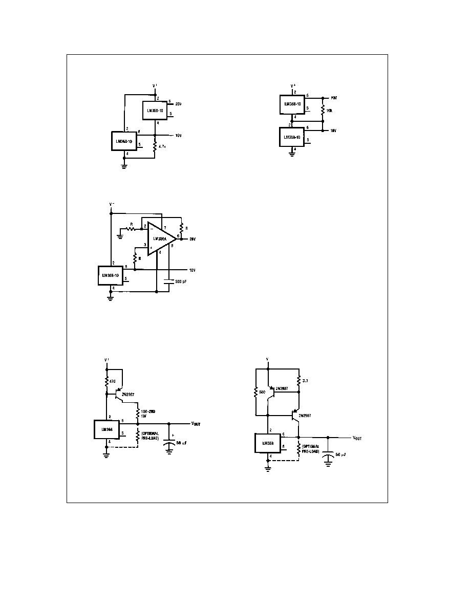
Typical Applications
(Continued)
Multiple Output Voltages
TL H 5522 ≠ 13
TL H 5522 ≠ 14
R
e
Thin Film Resistor Network
0 05% Matching and 5ppm Tracking
(Beckman 694-3-R-10K-A)
(Caddock T-914-10K-100-05)
or similar
TL H 5522 ≠ 15
Reference with Booster
TL H 5522 ≠ 16
100 mA Boosted Reference
TL H 5522 ≠ 17
5