
LM3814/LM3815
Fast Current Gauge IC with Ultra Low Loss Sense
Element and PWM Output
General Description
The LM3814/LM3815 Current Gauges provide easy to use
precision current measurement with virtually zero insertion
loss (typically 0.004
). The LM3814 is used for high-side
sensing and the LM3815 is used for low-side sensing.
A Delta Sigma analog to digital converter is incorporated to
precisely measure the current and to provide a current aver-
aging function. Current is averaged over 6 msec time peri-
ods in order to provide immunity to current spikes. The ICs
have a pulse-width modulated (PWM) output which indicates
the current magnitude and direction. The shutdown pin can
be used to inhibit false triggering during start-up, or to enter
a low quiescent current mode.
The LM3814 and LM3815 are factory-set in two different cur-
rent options. The sense range is -1A to +1A or -7A to +7A.
The user specifies a particular part number to match the cur-
rent range for a given application. The sampling interval for
these parts is 6ms. If larger sampling interval is desired for
better accuracy, please refer to the data sheets for the part
numbers LM3812 and LM3813.
Key Specifications
n
Ultra low insertion loss (typically 0.004
)
n
2V to 5.25V supply range
n
±
3.5% accuracy at room temperature (includes
accuracy of the internal sense element) (LM3814-1.0,
LM3815-1.0)
n
Low quiescent current in shutdown mode (typically 2.5
µA)
n
6 msec sampling interval
Features
n
No external sense element required
n
PWM output indicates the current magnitude and
direction
n
PWM output can be interfaced with microprocessors
n
Precision
current-sense technique
n
Low temperature sensitivity
n
Internal filtering rejects false trips
n
Internal Power-On-Reset (POR)
Applications
n
Battery charge/discharge gauge
n
Motion control diagnostics
n
Power supply load monitoring and management
n
Resettable smart fuse
Connection Diagrams
DS101013-1
Top View
LM3814
for High-Side Sensing
DS101013-3
Top View
LM3815
for Low-Side Sensing
January 1999
LM3814/LM3815
Fast
Current
Gauge
IC
with
Ultra
Low
Loss
Sense
Element
and
PWM
Output
© 1999 National Semiconductor Corporation
DS101013
www.national.com

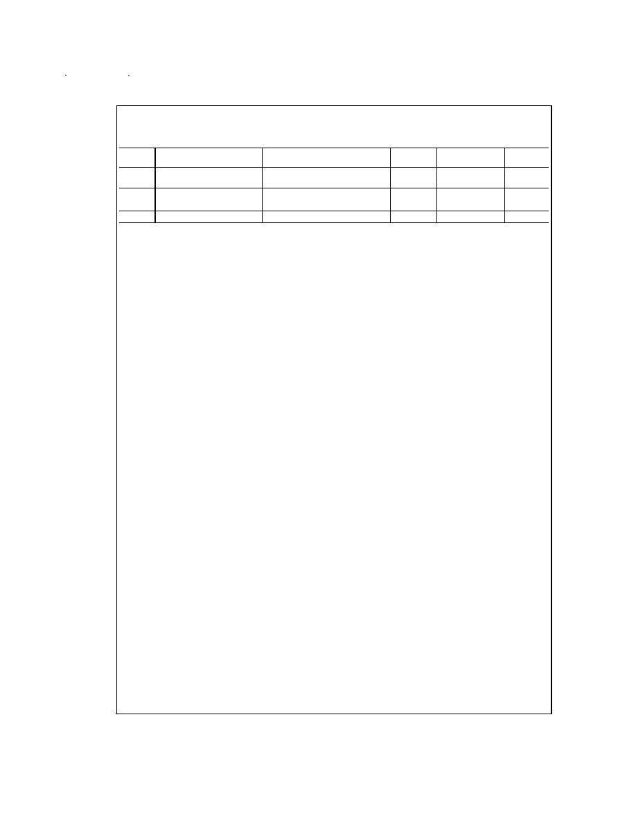
Ordering Information
Order No.
#
Sense
Range
Sampling
Interval
*
Sensing
Method
NS
Package
Number
Package
Type
Supplied As:
LM3814M-1.0
±
1A
6 ms
High-side
M08A
SO-8
95 units in Rails
LM3814MX-1.0
±
1A
6 ms
High-side
M08A
SO-8
2.5k units on Tape and Reel
LM3814M-7.0
±
7A
6 ms
High-side
M08A
SO-8
95 units in Rails
LM3814MX-7.0
±
7A
6 ms
High-side
M08A
SO-8
2.5k units on Tape and Reel
LM3815M-1.0
±
1A
6 ms
Low-side
M08A
SO-8
95 units in Rails
LM3815MX-1.0
±
1A
6 ms
Low-side
M08A
SO-8
2.5k units on Tape and Reel
LM3815M-7.0
±
7A
6 ms
Low-side
M08A
SO-8
95 units in Rails
LM3815MX-7.0
±
7A
6 ms
Low-side
M08A
SO-8
2.5k units on Tape and Reel
#
Suffix M indicates that the part is available in Surface Mount package. Suffix X indicates that the part is available in 2.5k units
on Tape and Reel.
*
Current is sampled over a fixed interval. The average current during this interval is indicated by the duty cycle of the PWM output
during next interval.
The Package code M08A is internal to National Semiconductor and indicates an 8-lead surface mount package, SO-8.
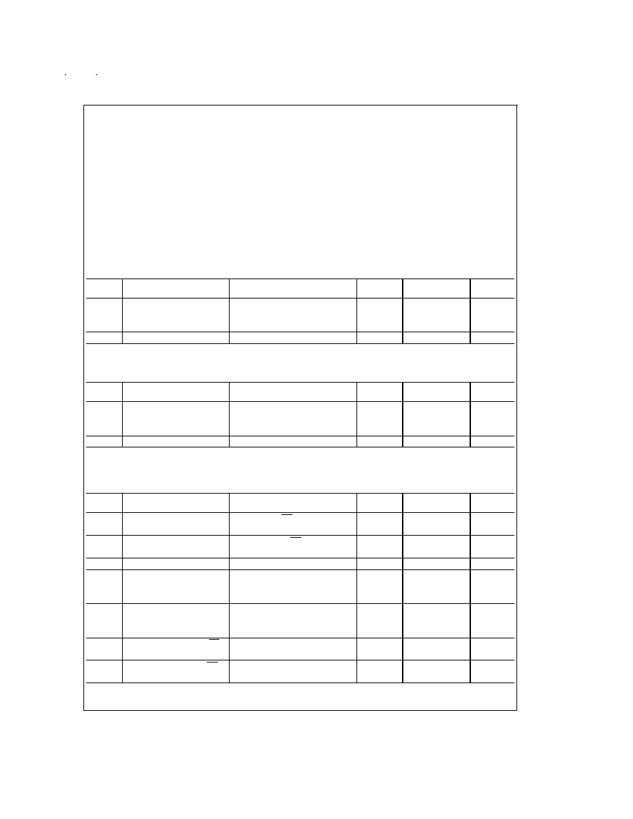
Pin Description (High-Side, LM3814)
Pin
Name
Function
1
SENSE+, V
DD
High side of internal current sense, also supply voltage.
2
SENSE-
Low side of internal current sense.
3
FLTR+
Filter input -- provides anti-aliasing for delta sigma modulator.
4
FLTR-
Filter input.
5
SD
Shutdown pin. Connected to V
DD
through a pull up resistor for normal operation.
When low, the IC goes into a low current mode (typically 3 µA).
6
PWM
PWM output indicates the current magnitude and direction.
7
GND
Ground
8
GND
Ground
Pin Description (Low-Side, LM3815)
Pin
Name
Function
1
SENSE+, GND
High side of internal current sense, also ground.
2
SENSE-
Low side of internal current sense.
3
FLTR+
Filter input ≠ provides anti-aliasing for delta sigma modulator.
4
FLTR-
Filter input.
5
SD
Shutdown pin. Connected to V
DD
through a pull up resistor for normal operation.
When low, the IC goes into a low current mode (typically 3 µA).
6
PWM
PWM output indicates the current magnitude and direction.
7
GND
Ground
8
V
DD
V
DD
(supply)
www.national.com
2
Absolute Maximum Ratings
(Note 1)
If Military/Aerospace specified devices are required,
please contact the National Semiconductor Sales Office/
Distributors for availability and specifications.
Absolute Maximum Supply Voltage
5.5V
Power Dissipation
(Note 2)
ESD Susceptibility (Note 3)
1.5 kV
Sense Current (peak, for 200 msec) (Note 4)
10A
Sink Current for PWM pin
1 mA
Voltage on Pin 5
5.25V
Maximum Junction Temperature
150∞C
Storage Temperature
-65∞C to +150∞C
Lead Temperature (Soldering, 10 sec)
260∞C
Operating Ratings
(Note 1)
Input Voltage
2.0V to 5.25V
Sense Current (continuous) (Note 4)
7A
Junction Temperature Range
-40∞C to +125∞C
Electrical Characteristics
LM3814-1.0, LM3815-1.0
V
DD
= 5.0V for the following specifications. Supply bypass capacitor is 1µF and filter capacitor is 0.1µF.
Symbol
Parameter
Conditions
Typ
(Note 5)
Limit
(Note 6)
Units
I
ACC
Average Current Accuracy
(Note 7)
at 0.9A current
0.9
A
0.868 / 0.850
A (min)
0.932 / 0.950
A (max)
e
n
Effective Output Noise (rms)
12
mA
LM3814-7.0, LM3815-7.0
V
DD
= 5.0V for the following specifications. Supply bypass capacitor is 1µF and filter capacitor is 0.1µF.
Symbol
Parameter
Conditions
Typ
(Note 5)
Limit
(Note 6)
Units
I
ACC
Average Current Accuracy
(Note 7)
at 2.5A current (Note 8)
2.5
A
2.350 / 2.288
A (min)
2.650 / 2.712
A (max)
e
n
Effective Output Noise (rms)
120
mA
Common Device Parameters
Unless otherwise specified, V
DD
= 5.0V for the following specifications. Supply bypass capacitor is 1µF and filter capacitor is
0.1µF.
Symbol
Parameter
Conditions
Typ
(Note 5)
Limit
(Note 6)
Units
I
Q1
Quiescent Current
Normal Mode, SD = high
100
µA
160
µA (max)
I
Q2
Quiescent Current
Shutdown Mode, SD = low
2.5
µA
10
µA (max)
D
RES
PWM Resolution
0.8
%
t
S
Sampling Time
6
ms
4
ms (min)
10
ms (max)
f
P
Frequency of PWM Waveform
160
Hz
100
Hz (min)
250
Hz (max)
V
TH
Threshold High Level for SD
1.2
V
1.8
V (min)
V
TL
Threshold Low Level for SD
1.3
V
0.7
V (max)
www.national.com
3
Common Device Parameters
(Continued)
Unless otherwise specified, V
DD
= 5.0V for the following specifications. Supply bypass capacitor is 1µF and filter capacitor is
0.1µF.
Symbol
Parameter
Conditions
Typ
(Note 5)
Limit
(Note 6)
Units
V
OH
Logic High Level for PWM
Load current = 1mA, 2V
V
DD
5.25V
V
DD
- 0.05
V
DD
- 0.2
V
V (min)
V
OL
Logic Low Level for PWM
Sink current = 1mA, 2V
V
DD
5.25V
0.04
V
0.2
V (max)
P
I
Insertion Loss
I
SENSE
= 1A (Note 9)
0.004
Note 1: Absolute Maximum Ratings indicate limits beyond which damage to the device may occur. Operating Ratings indicate conditions for which the device is in-
tended to be functional, but do not guarantee specific performance limits. For guaranteed specifications and test conditions, see Electrical Characteristics. The guar-
anteed specifications apply only for the test conditions listed. Some performance characteristics may degrade when the device is not operated under the listed test
conditions.
Note 2: At elevated temperatures, devices must be derated based on package thermal resistance. The device in the surface-mount package must be derated at
JA
= 150∞C/W (typically), junction-to-ambient.
Note 3: The human body model is a 100 pF capacitor discharged through a 1.5 k
resistor into each pin.
Note 4: The absolute maximum peak and continuous currents specified are not tested. These specifications are dependent on the
JA
, which is 150∞C/W for the S08
package.
Note 5: Typical numbers are at 25∞C and represent the most likely parametric norm. Specifications in standard type face are for T
J
= 25∞C and those with boldface
type apply over full operating temperature ranges.
Note 6: Limits are 100% production tested at 25∞C. Limits over the operating temperature range are guaranteed through correlation using Statistical Quality Control
(SQC) methods. The limits are used to calculate National's Averaging Outgoing Quality Level (AOQL).
Note 7: There is a variation in accuracy over time due to thermal effects. Please refer to the PWM Output and Current Accuracy section for more information.
Note 8: The PWM accuracy for LM3814-7.0 and LM3815-7.0 depends on the amount of copper area under pins 1 and 2, and the layout. Please refer to the 'PWM
Output and Current Accuracy' section for more information.
Note 9: The tolerance of the internal lead frame resistor is corrected internally. The temperature coefficient of this resistor is 2600 ppm/∞C.
www.national.com
4
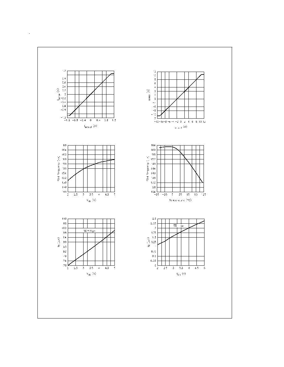
Typical Performance Characteristics
Supply bypass capacitor is 0.1µF and filter capacitor is 0.1µF.
Measured Current vs Actual Current
(LM3814-1.0 and LM3815-1.0)
DS101013-15
Measured Current vs Actual Current
(LM3814-7.0 and LM3815-7.0)
DS101013-24
PWM Frequency vs Supply Voltage
DS101013-14
PWM Frequency vs Temperature
DS101013-17
Operating Current vs Supply Voltage
DS101013-18
Shutdown Current vs Supply Voltage
DS101013-19
www.national.com
5