LM3822
Precision Current Gauge IC with Internal Zero Ohm
Sense Element and PWM Output
General Description
The LM3822 Current Gauge provides easy to use precision
current measurement with virtually zero insertion loss (typi-
cally 0.003
). The LM3822 is used for high-side sensing.
A Delta Sigma analog to digital converter is incorporated to
precisely measure the current and to provide a current aver-
aging function. Current is averaged over 50 msec time peri-
ods in order to provide immunity to current spikes. The ICs
have a pulse-width modulated (PWM) output which indicates
the current magnitude and direction. The shutdown pin can
be used to inhibit false triggering during start-up, or to enter
a low quiescent current mode.
The LM3822 is factory-set in two different current options.
The sense range is -1.0A to +1.0A or -2.0A to +2.0A. The
sampling interval for this part is 50ms. If faster sampling is
desired, please refer to the data sheet for the part number
LM3824.
Key Specifications
n
Ultra low insertion loss (typically 0.003
)
n
2V to 5.5V supply range
n
±
2% accuracy at room temperature for the 1A device
(includes accuracy of the internal sense element)
n
Low quiescent current in shutdown mode (typically
1.8 µA)
n
50 msec sampling interval
n
In MSOP-8 Package
Features
n
No external sense element required
n
PWM output indicates the current magnitude and
direction
n
PWM output is easily interfaced with microprocessors
and controllers
n
Precision
current-sense technique
n
Low temperature sensitivity
n
Internal filtering rejects false trips
n
Internal Power-On-Reset (POR)
n
DC Offset is less than 1 mA for 1A part
Applications
n
Battery charge/discharge gauge
n
Motion control diagnostics
n
Power supply load monitoring and management
n
Resettable smart fuse
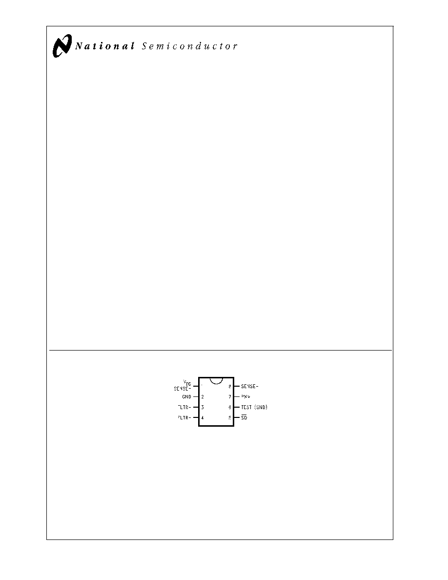
Connection Diagram
DS101249-1
Top View
LM3822 for High-Side Sensing
July 2000
LM3822
Precision
Current
Gauge
IC
with
Internal
Zero
Ohm
Sense
Element
and
PWM
Output
© 2000 National Semiconductor Corporation
DS101249
www.national.com

Ordering Information
Order No.
*
Sense
Range
Sampling
Interval
*
Sensing
Method
NS
Package
Number
Package
Type
Supplied As:
LM3822MM-1.0
±
1.0A
50 ms
High-side
MUA08A
MSOP-8
Tape and Reel
(1000 units/reel)
LM3822MMX-1.0
±
1.0A
50 ms
High-side
MUA08A
MSOP-8
Tape and Reel
(3500 units/reel)
LM3822MM-2.0
±
2.0A
50 ms
High-side
MUA08A
MSOP-8
Tape and Reel
(1000 units/reel)
LM3822MMX-2.0
±
2.0A
50 ms
High-side
MUA08A
MSOP-8
Tape and Reel
(3500 units/reel)
*
Current is sampled over a fixed interval. The average current during this interval is indicated by the duty cycle of the PWM output
during next interval.
Pin Description (High-Side, LM3822)
Pin
Name
Function
1
SENSE+, V
DD
High side of internal current sense, also supply voltage.
2
GND
Supply Ground.
3
FLTR+
Filter input -- provides anti-aliasing for delta sigma modulator.
4
FLTR-
Filter input.
5
SD
Shutdown input. Connected to V
DD
through a pull-up resistor for normal operation.
When low, the LM3822 is put into a low current mode.
6
TEST
Connect to GND for normal operation.
7
PWM
Digital output indicates the current magnitude and direction.
8
SENSE-
Low side of internal current sense.
LM3822
www.national.com
2

Absolute Maximum Ratings
(Note 1)
If Military/Aerospace specified devices are required,
please contact the National Semiconductor Sales Office/
Distributors for availability and specifications.
Absolute Maximum Supply Voltage
5.5V
Power Dissipation
(Note 2)
ESD Susceptibility (Note 3)
1.5 kV
Sense Current (peak, for 200 msec) (Note 4)
10A
Sink Current for PWM pin
1mA
Maximum Junction Temperature
150∞C
Storage Temperature
-65∞C to +150∞C
Lead Temperature (Soldering, 10 sec)
260∞C
Operating Ratings
(Note 1)
Input Voltage
2.0V to 5.25V
Sense Current (continuous) (Note 4)
5A
Junction Temperature Range
-40∞C to +85∞C
Electrical Characteristics
Typical numbers are at 25∞C and represent the most likely parametric norm.
Specifications in standard type face are for T
J
= 25∞C and those with boldface type apply over full operating temperature
ranges.
LM3822-1.0
SENSE+V
DD
= 3.6V for the following specifications. Supply bypass capacitor is 1 µF and filter capacitor is 0.1 µF.
Symbol
Parameter
Conditions
Typ
(Note 5)
Limit
(Note 6)
Units
I
ACC
Average Current Accuracy
(Note 7)
1.0A current
1.0
A
0.98 / 0.96
A (min)
1.02 / 1.04
A (max)
e
n
Effective Output Noise (rms)
2
mA
LM3822-2.0
SENSE+V
DD
= 3.6V for the following specifications. Supply bypass capacitor is 1 µF and filter capacitor is 0.1 µF.
Symbol
Parameter
Conditions
Typ
(Note 5)
Limit
(Note 6)
Units
I
ACC
Average Current Accuracy
(Note 7)
2.0A current (Note 8)
2.0
A
1.94 / 1.90
A (min)
2.06 / 2.10
A (max)
e
n
Effective Output Noise (rms)
6
mA
Common Device Parameters
Unless otherwise specified, V
DD
= 3.6V for the following specifications. Supply bypass capacitor is 1 µF and filter capacitor is
0.1 µF.
Symbol
Parameter
Conditions
Typ
(Note 5)
Limit
(Note 6)
Units
I
Q1
Quiescent Current
Normal Mode, SD = high
95
µA
150
µA (max)
I
Q2
Quiescent Current
Shutdown Mode, SD = low
1.8
µA
10
µA (max)
D
RES
PWM Resolution
0.1
%
t
S
Sampling Time
50
ms
40
ms (min)
80
ms (max)
f
P
Frequency of PWM Waveform
20
Hz
12.5
Hz (min)
25
Hz (max)
V
TH
Threshold High Level for SD
1.3
V
1.8
V (min)
LM3822
www.national.com
3

Common Device Parameters
(Continued)
Unless otherwise specified, V
DD
= 3.6V for the following specifications. Supply bypass capacitor is 1 µF and filter capacitor is
0.1 µF.
Symbol
Parameter
Conditions
Typ
(Note 5)
Limit
(Note 6)
Units
V
TL
Threshold Low Level for SD
1.2
V
0.7
V (max)
V
OH
Logic High Level for PWM
Load current = 1 mA, 2V
V
DD
5.25V
V
DD
- 0.05
V
DD
- 0.2
V
V (min)
V
OL
Logic Low Level for PWM
Sink current = 1 mA, 2V
V
DD
5.25V
0.04
V
0.2
V (max)
P
I
Insertion Loss
I
SENSE
= 1A (Note 9)
0.003
Note 1: Absolute Maximum Ratings indicate limits beyond which damage to the device may occur. Operating Ratings indicate conditions for which the device is in-
tended to be functional, but do not guarantee specific performance limits. For guaranteed specifications and test conditions, see Electrical Characteristics. The guar-
anteed specifications apply only for the test conditions listed. Some performance characteristics may degrade when the device is not operated under the listed test
conditions.
Note 2: At elevated temperatures, devices must be derated based on package thermal resistance. The device in the surface-mount package must be derated at
JA
= 220∞C/W (typically), junction-to-ambient.
Note 3: The human body model is a 100 pF capacitor discharged through a 1.5 k
resistor into each pin.
Note 4: The absolute maximum peak and continuous currents specified are not tested. These specifications are dependent on the
JA
, which is 220∞C/W for the
MSOP-8 package.
Note 5: Typical numbers are at 25∞C and represent the most likely parametric norm. Specifications in standard type face are for T
J
= 25∞C and those with boldface
typeapply over full operating temperature ranges.
Note 6: Limits are 100% production tested at 25∞C. Limits over the operating temperature range are guaranteed through correlation using Statistical Quality Control
(SQC) methods. The limits are used to calculate National's Average Outgoing Quality Level (AOQL).
Note 7: There is a variation in accuracy over time due to thermal effects. Please refer to the "PWM Output and Current Accuracy" section for more information.
Note 8: This parameter is production tested at 1A and guaranteed by design at 2A.
Note 9: The tolerance of the internal lead frame resistor is corrected internally. The temperature coefficient of this resistor is 2600 ppm/∞C.
LM3822
www.national.com
4

Typical Performance Characteristics
Supply bypass capacitor is 0.1 µF and filter capacitor is 0.1 µF.
Measured Current vs Actual Current
(LM3822-1.0)
DS101249-24
Measured Current vs Actual Current
(LM3822-2.0)
DS101249-25
PWM Frequency vs Supply Voltage
DS101249-33
PWM Frequency vs Temperature
DS101249-23
Operating Current vs Supply Voltage
DS101249-18
Shutdown Current vs Supply Voltage
DS101249-20
LM3822
www.national.com
5
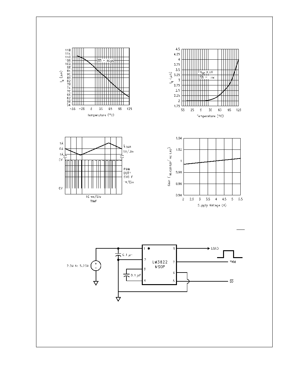
Typical Performance Characteristics
Supply bypass capacitor is 0.1 µF and filter capacitor is
0.1 µF. (Continued)
Note 10: These curves represent a statistical average such that the noise is insignificant.
Typical Application Circuits
In the application circuits, the 0.1 µF ceramic capacitor between pins 1 and 2
is used for bypassing, and the 0.1 µF ceramic capacitor between pins 3 and 4 is used for filtering. Shutdown (SD) is tied to
V
DD
through a 10 k
resistor.
Operating Current vs Temperature
DS101249-19
Shutdown Current vs Temperature
DS101249-21
Current vs PWM Duty Cycle
DS101249-22
Accuracy vs Supply Voltage
DS101249-28
DS101249-5
FIGURE 1. High Side Sense
LM3822
www.national.com
6

Typical Application Circuits
In the application circuits, the 0.1 µF ceramic capacitor between pins 1 and 2
is used for bypassing, and the 0.1 µF ceramic capacitor between pins 3 and 4 is used for filtering. Shutdown (SD) is tied to
V
DD
through a 10 k
resistor. (Continued)
DS101249-7
FIGURE 2. Paralleling LM3822 for Higher Load Current
I
TOTAL
= 2.2(D
1
-0.5)I
MAX
+ 2.2(D
2
-0.5)I
MAX
where D
1
is the duty cycle of PWM1 and D
2
is the duty cycle of PWM2.
Please refer to the Product Operation section for more information.
DS101249-8
FIGURE 3. High Voltage Operation -- V
IN
Greater Than 5.5V (High Side Sense)
(PWM output is referred to Pin 6)
LM3822
www.national.com
7
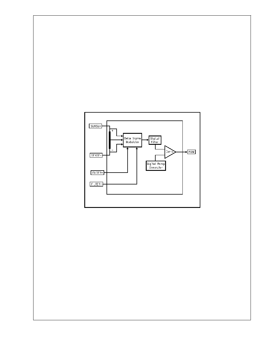
Product Operation
The current is sampled by the delta-sigma modulator, as il-
lustrated in
Figure 4. The pulse density output of the
delta-sigma modulator is digitally filtered. The digital output
is then compared to the output of a digital ramp generator.
This produces a PWM output. The duty cycle of the PWM
output is proportional to the amount of current flowing. A duty
cycle of 50% indicates zero current flow. If the current is flow-
ing in positive direction, the duty cycle will be greater than
50%. Conversely, the duty cycle will be less than 50% for
currents flowing in the negative direction. A duty cycle of
95.5% (4.5%) indicates the current is at I
MAX
(-I
MAX
). The IC
can sense currents from -I
MAX
to +I
MAX
. Options for I
MAX
are
1.0A or 2.0A. The sense current is given by:
I
SENSE
= 2.2 (D-0.5)(I
MAX
)
where D is the duty cycle of the PWM waveform, and I
MAX
is
the full scale current (1.00A or 2.00A). Similarly, the duty
cycle is given by:
D = [I
SENSE
/(2.2 I
MAX
)] + 0.5
For quick reference, see the Conversion Table in
Table 1.
In this IC, the current is averaged over 50 msec time slots.
Hence, momentary current surges of less than 50 msec are
tolerated.
This is a sampled data system which requires an
anti-aliasing filter, provided by the filter capacitor.
The delta-sigma modulator converts the sensed current to
the digital domain. This allows digital filtering, and provides
immunity to current and noise spikes. This type of filtering
would be difficult or impossible to accomplish on an IC with
analog components.
The user also needs to specify the full scale value. See the
Ordering Information table for details.
DS101249-10
FIGURE 4. Functional block diagram of LM3822
LM3822
www.national.com
8

PWM Output and Current
Accuracy
Offset
The PWM output is quantized to 1024 levels. Therefore, the
duty cycle can change only in increments of 1/1024.
There is a one-half (0.5) quantization cycle delay in the out-
put of the PWM circuitry. That is to say that instead of a duty
cycle of N/1024, the duty cycle actually is (N+
1
/
2
)/1024.
The quantization error can be corrected for if a more precise
result is desired. To correct for this error, simply subtract
1/2048 from the measured duty cycle.
The extra half cycle delay will show up as a DC offset of
1
/
2
bit if it is not corrected for. This is approximately 1.0 mA for
1.0 Amp parts, and 10 mA for 2.0 Amp parts.
Jitter
In addition to quantization, the duty cycle will contain some
jitter. The jitter is quite small (for example, the standard de-
viation of jitter is only 0.1% for the LM3822-1.0). Statistically
the jitter can cause an error in a current sample. Because the
jitter is a random variable, the mean and standard deviation
are used. The mean, or average value, of the jitter is zero.
The standard deviation (0.1%) can be used to define the
peak error caused from jitter.
The "crest factor" has often been used to define the maxi-
mum error caused by jitter. The crest factor defines a limit
within which 99.7% of the samples fall. The crest factor is de-
fined as
±
0.3% error in the duty cycle.
Since the jitter is a random variable, averaging multiple out-
puts will reduce the effective jitter. Obeying statistical laws,
the jitter is reduced by the square root of the number of read-
ings that are averaged. For example, if four readings of the
duty cycle are averaged, the resulting jitter (and crest factor)
are reduced by a factor of two.
Jitter and Noise
Jitter in the PWM output appears as noise in the current
measurement. The Electrical Characteristics show noise
measured in current RMS (root mean square). Arbitrarily one
could specify PWM jitter, as opposed to noise. In either case
the effect results in a random error in an individual current
measurement.
Noise, just like jitter, can be reduced by averaging many
readings. The RMS value of the noise corresponds to one
standard deviation. The "crest factor" can be calculated in
terms of current, and is equal to
±
3 sigma (RMS value of the
noise).
Noise will also be reduced by averaging multiple readings,
and follows the statistical laws of a random variable.
Accuracy versus Noise
The graph shown in
Figure 5 illustrates the typical response
of
±
1 Ampere current gauges. In this graph, the horizontal
axis indicates time, and the vertical axis indicates measured
current (the PWM duty cycle has been converted to current).
The graph was generated for an actual current of 500 mA.
The difference between successive readings manifests itself
as jitter in the PWM output or noise in the current measure-
ment (when duty cycle of the PWM output is converted to
current).
The accuracy of the measurement depends on the noise in
the current waveform. The accuracy can be improved by av-
eraging several outputs. Although there is variation in suc-
cessive readings, a very accurate measurement can be ob-
tained by averaging the readings. For example, on
averaging the readings shown in this example, the average
current measurement is 502.3 mA (
Figure 5). This value is
very close to the actual value of 500 mA. Moreover, the ac-
curacy depends on the number of readings that are
averaged.
Low Current Measurements
The DC offset of the LM3822-1.0 is typically under 1 mA.
This low offset allows accurate low current measurements.
Even currents in the 10 mA range can be measured with ac-
curacies typically better than
±
5%.
DS101249-26
FIGURE 5. Typical Response of LM3822
LM3822
www.national.com
9
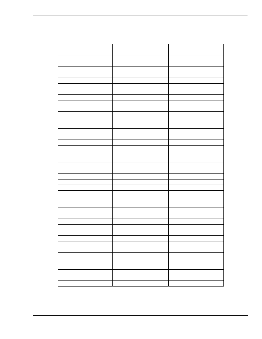
Look-Up Tables
The following tables show how to convert the duty cycle of
the PWM output to a current value, and vice versa. The
quantization error of
1
/
2
bit is not shown in these tables.
Please see the "PWM Output and Current Accuracy" section
for more details.
TABLE 1. Current to Duty Cycle Conversion Table
Sense Current
(Imax = 1.0A)
Sense Current
(Imax = 2.0A)
Duty Cycle (%)
1
2
95.5
0.95
1.90
93.2
0.90
1.80
90.9
0.85
1.70
88.6
0.80
1.60
86.4
0.75
1.50
84.1
0.70
1.40
81.8
0.65
1.30
79.5
0.60
1.20
77.3
0.55
1.10
75.0
0.50
1
72.7
0.45
0.90
70.5
0.40
0.80
68.2
0.35
0.70
65.9
0.30
0.60
63.6
0.25
0.50
61.4
0.20
0.40
59.1
0.15
0.30
56.8
0.10
0.20
54.5
0.05
0.10
52.3
0.00
0.00
50
-0.05
-0.10
47.7
-0.10
-0.20
45.5
-0.15
-0.30
43.2
-0.20
-0.40
40.9
-0.25
-0.50
38.6
-0.30
-0.60
36.4
-0.35
-0.70
34.1
-0.40
-0.80
31.8
-0.45
-0.90
29.5
-0.50
-1
27.3
-0.55
-1.10
25
-0.60
-1.20
22.7
-0.65
-1.30
20.5
-0.70
-1.40
18.2
-0.75
-1.50
15.9
-0.80
-1.60
13.6
-0.85
-1.70
11.4
-0.90
-1.80
9.1
-0.95
-1.90
6.8
-1
-2
4.5
LM3822
www.national.com
10
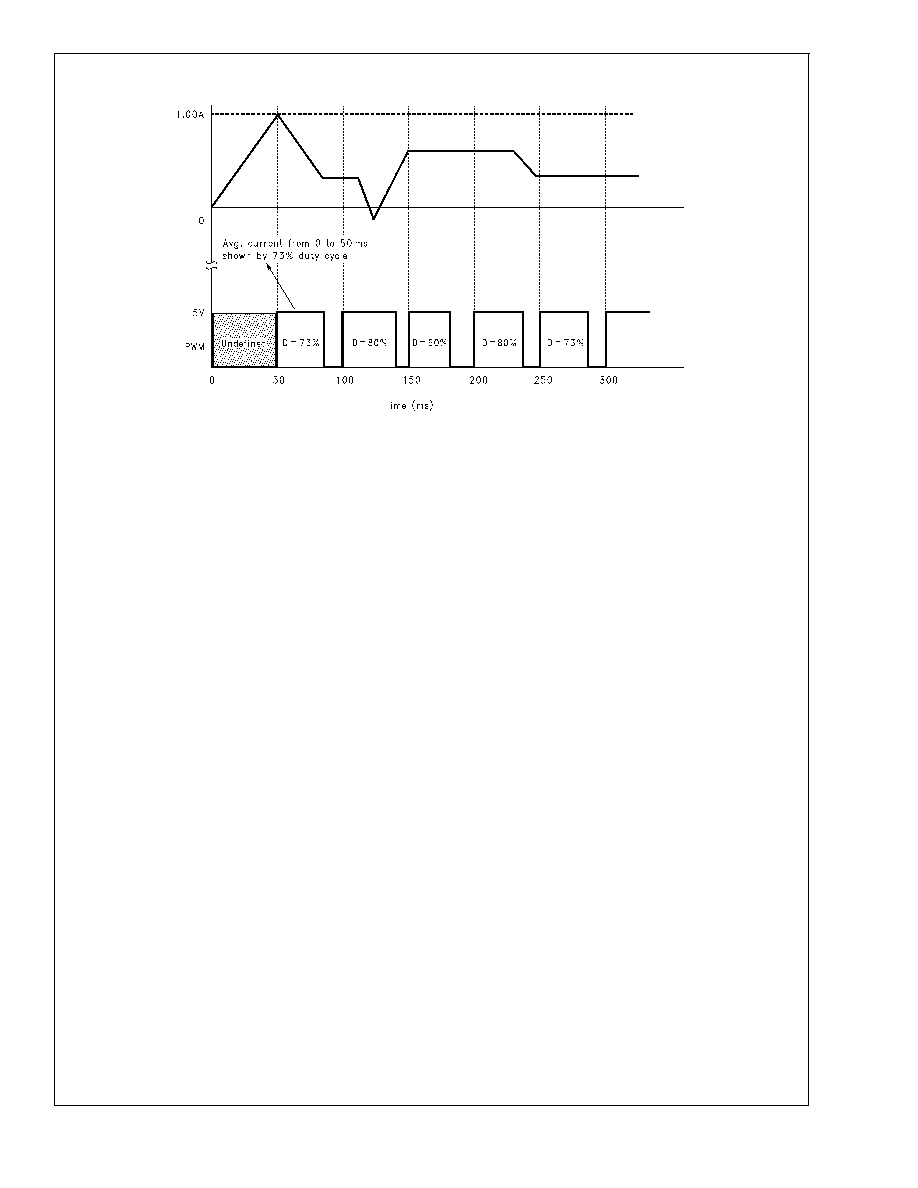
Timing Diagram
DS101249-11
Duty cycle of the PWM waveform during any sampling interval indicates the current magnitude (average) and direction during the previous sampling interval.
FIGURE 6. Typical Timing Diagram for Mostly Positive Current
LM3822
www.national.com
11

Physical Dimensions
inches (millimeters) unless otherwise noted
LIFE SUPPORT POLICY
NATIONAL'S PRODUCTS ARE NOT AUTHORIZED FOR USE AS CRITICAL COMPONENTS IN LIFE SUPPORT
DEVICES OR SYSTEMS WITHOUT THE EXPRESS WRITTEN APPROVAL OF THE PRESIDENT AND GENERAL
COUNSEL OF NATIONAL SEMICONDUCTOR CORPORATION. As used herein:
1. Life support devices or systems are devices or
systems which, (a) are intended for surgical implant
into the body, or (b) support or sustain life, and
whose failure to perform when properly used in
accordance with instructions for use provided in the
labeling, can be reasonably expected to result in a
significant injury to the user.
2. A critical component is any component of a life
support device or system whose failure to perform
can be reasonably expected to cause the failure of
the life support device or system, or to affect its
safety or effectiveness.
National Semiconductor
Corporation
Americas
Tel: 1-800-272-9959
Fax: 1-800-737-7018
Email: support@nsc.com
National Semiconductor
Europe
Fax: +49 (0) 180-530 85 86
Email: europe.support@nsc.com
Deutsch Tel: +49 (0) 69 9508 6208
English
Tel: +44 (0) 870 24 0 2171
FranÁais Tel: +33 (0) 1 41 91 8790
National Semiconductor
Asia Pacific Customer
Response Group
Tel: 65-2544466
Fax: 65-2504466
Email: ap.support@nsc.com
National Semiconductor
Japan Ltd.
Tel: 81-3-5639-7560
Fax: 81-3-5639-7507
www.national.com
8-Lead MSOP
See Ordering Information table for Order Numbers
NS Package Number MUA08A
LM3822
Precision
Current
Gauge
IC
with
Internal
Zero
Ohm
Sense
Element
and
PWM
Output
National does not assume any responsibility for use of any circuitry described, no circuit patent licenses are implied and National reserves the right at any time without notice to change said circuitry and specifications.