 | –≠–ª–µ–∫—Ç—Ä–æ–Ω–Ω—ã–π –∫–æ–º–ø–æ–Ω–µ–Ω—Ç: LM3875DWF | –°–∫–∞—á–∞—Ç—å:  PDF PDF  ZIP ZIP |
LM3875
Overture
TM
Audio Power Amplifier Series
High-Performance 56W Audio Power Amplifier
General Description
The LM3875 is a high-performance audio power amplifier
capable of delivering 56W of continuous average power to
an 8
load with 0.1% THD+N from 20Hz to 20kHz.
The performance of the LM3875, utilizing its Self Peak In-
stantaneous Temperature (∞Ke) (SPiKe
TM
) protection cir-
cuitry, puts it in a class above discrete and hybrid amplifiers
by providing an inherently, dynamically protected Safe Oper-
ating Area (SOA). SPiKe protection means that these parts
are completely safeguarded at the output against overvolt-
age, undervoltage, overloads, caused by shorts to the sup-
plies, thermal runaway, and instantaneous temperature
peaks.
The LM3875 maintains an excellent signal-to-noise ratio of
greater than 95dB(min) with a typical low noise floor of
2.0µV. It exhibits extremely low THD+N values of 0.06% at
the rated output into the rated load over the audio spectrum,
and provides excellent linearity with an IMD (SMPTE) typical
rating of 0.004%.
Features
n
56W continuous average output power into 8
n
100W instantaneous peak output power capability
n
Signal-to-Noise Ratio
>
95dB (min)
n
Output protection from a short to ground or to the
supplies via internal current limiting circuitry
n
Output over-voltage protection against transients from
inductive loads
n
Supply under-voltage protection, not allowing internal
biasing to occur when |V+| + |V-|
12V, thus eliminating
turn-on and turn-off transients
n
11 lead TO-220 package
n
Wide supply voltage range: |V+| + |V-| = 20V to 84V
Applications
n
Component or compact stereos
n
Self-powered speakers
n
Surround-sound amplifiers
n
High-end stereo TVs
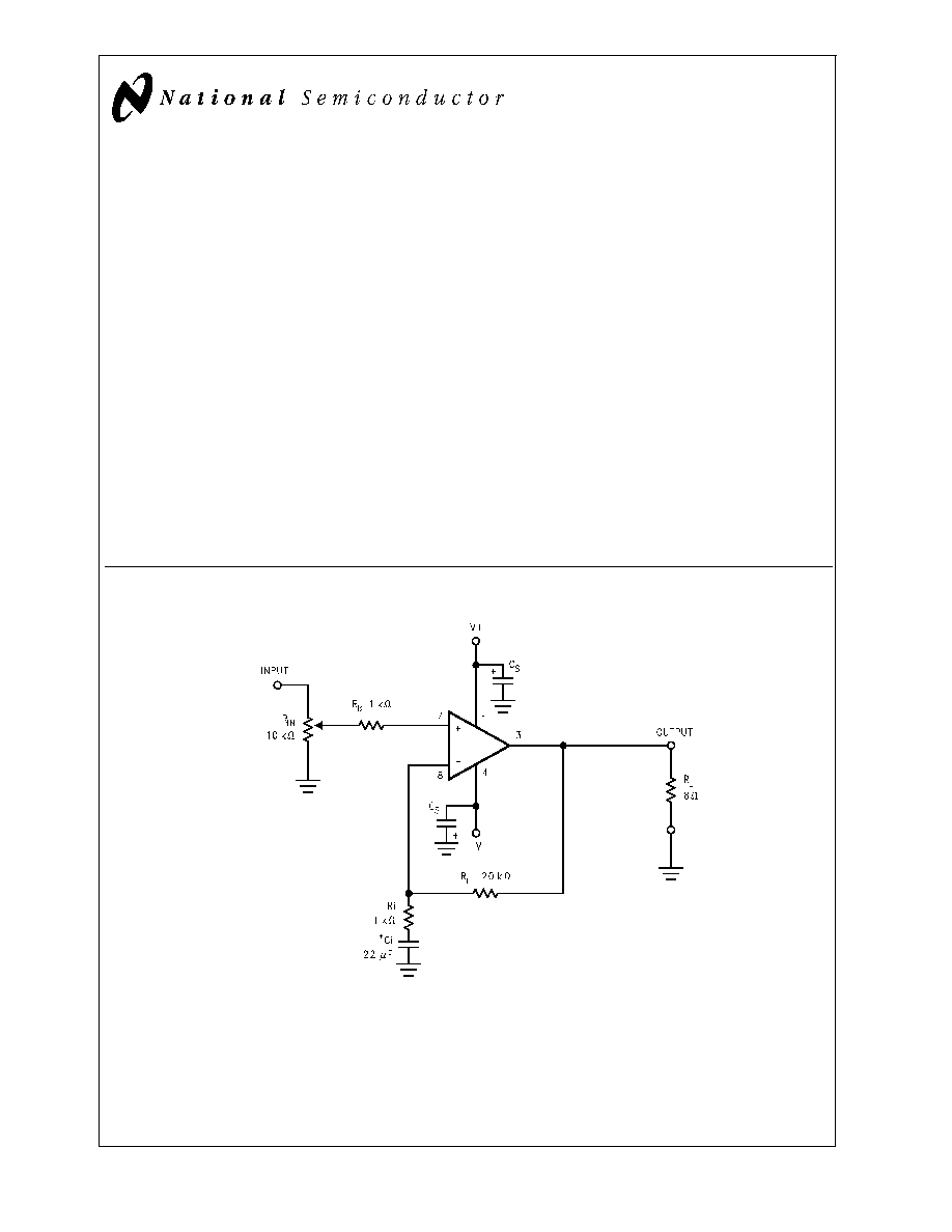
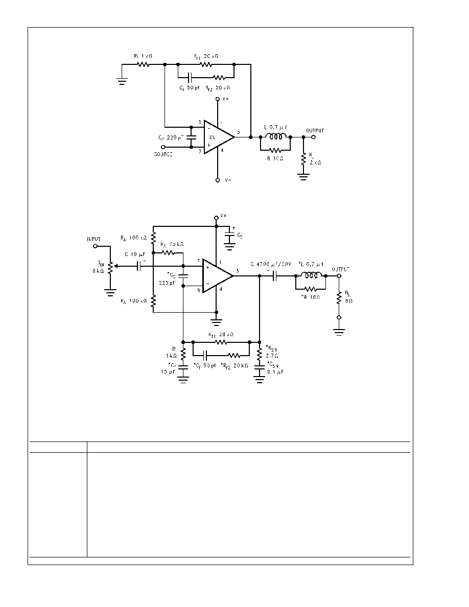
Typical Application
Overture
TM
and SPiKe
TM
are trademarks of National Semiconductor Corporation.
DS011449-1
*Optional components dependent upon specific design requirements. Refer to the External Components Description section for a component function
description.
FIGURE 1. Typical Audio Amplifier Application Circuit
August 2000
LM3875
Overture
Audio
Power
Amplifier
Series
High-Performance
56W
Audio
Power
Amplifier
© 2000 National Semiconductor Corporation
DS011449
www.national.com
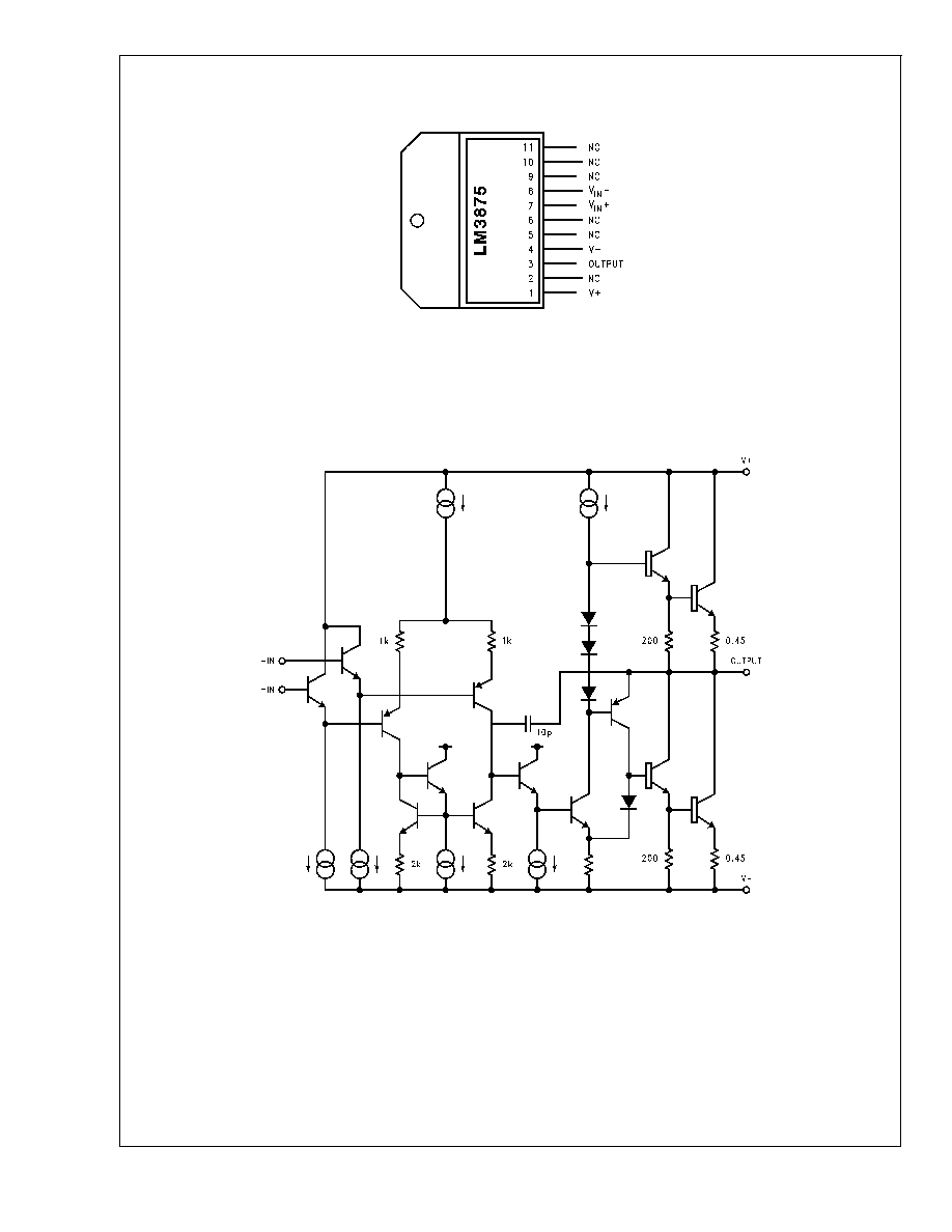
Connection Diagram
Equivalent Schematic
(Excluding active protection circuitry)
Plastic Package (Note 8)
DS011449-2
Top View
Order Number LM3875T or LM3875TF
See NS Package Number TA11B for
Staggered Lead Non-Isolated Package
or TF11B for Staggered Lead Isolated Package
DS011449-6
LM3875
www.national.com
2
Absolute Maximum Ratings
(Notes 1, 2)
If Military/Aerospace specified devices are required,
please contact the National Semiconductor Sales Office/
Distributors for availability and specifications.
Supply Voltage |V
+
| + |V
-
| (No Signal)
94V
Supply Voltage |V
+
| + |V
-
| (Input Signal)
84V
Common Mode Input Voltage
(V
+
or V
-
) and
|V
+
| + |V
-
|
80V
Differential Input Voltage
60V
Output Current
Internally Limited
Power Dissipation (Note 3)
125W
ESD Susceptibility (Note 4)
2500V
Junction Temperature (Note 5)
150∞C
Soldering Information
T package (10 seconds)
260∞C
Storage Temperature
-40∞C to +150∞C
Thermal Resistance
JC
1∞C/W
JA
43∞C/W
Operating Ratings
(Notes 1, 2)
Temperature Range
T
MIN
T
A
T
MAX
-20∞C
T
A
+85∞C
Supply Voltage |V
+
| + |V
-
|
20V to 84V
Note: Operation is guaranteed up to 84V, however, distortion may be intro-
duced from the SPiKe Protection Circuitry when operating above 70V if
proper thermal considerations are not taken into account. Refer to the Ther-
mal Considerations section for more information. (See SPiKe Protection Re-
sponse)
Electrical Characteristics
(Notes 1, 2)
The following specifications apply for V
+
= +35V, V
-
= -35V with R
L
= 8
unless otherwise specified. Limits apply for T
A
=
25∞C.
Symbol
Parameter
Conditions
LM3875
Units
(Limits)
Typical
(Note 6)
Limit
(Note 7)
|V
+
| + |V
-
|
Power Supply Voltage
20
84
V (Min)
V (Max)
**P
O
Output Power (Continuous Average)
THD + N = 0.1% (Max)
f = 1 kHz, f = 20 kHz
56
40
W (Min)
Peak P
O
Instantaneous Peak Output Power
100
W
THD + N
Total Harmonic Distortion Plus Noise
40W, 20 Hz
f
20 kHz
A
V
= 26 dB
0.06
%
**SR
Slew Rate (Note 9)
V
IN
= 1.414 Vrms, f = 10 kHz
Square-wave, R
L
= 2 k
11
5
V/µs
(Min)
*I+
Total Quiescent Power Supply
Current
V
CM
= 0V, V
O
= 0V, I
o
= 0 mA
30
70
mA
(Max)
*V
OS
Input Offset Voltage
V
CM
= 0V, I
o
= 0 mA
1
10
mV
(Max)
I
B
Input Bias Current
V
CM
= 0V, I
o
= 0 mA
0.2
1
µA
(Max)
I
OS
Input Offset Current
V
CM
= 0V, I
o
= 0 mA
0.01
0.2
µA
(Max)
I
o
Output Current Limit
|V
+
| = |V
-
| = 10V, t
on
= 10 ms, V
O
= 0V
6
4
A(Min)
*V
od
Output Dropout Voltage
|V
+
-V
o
-
|, V
+
= 20V, I
o
= +100 mA
|V
o
-V
-
|, V
-
= -20V, I
o
= -100 mA
1.6
2.7
5
5
V (Max)
V (Max)
*PSRR
Power Supply Rejection Ratio
V
+
= 40V to 20V, V
-
= -40V,
V
cm
= 0V, I
o
= 0 mA
V
+
= 40V, V = -40V to -20V,
V
cm
= 0V, I
o
= 0 mA
120
120
85
85
dB (Min)
*CMRR
Common Mode Rejection Ratio
V
+
= 60V to 20V, V
-
= -20V to -60V,
V
cm
= 20V to -20V, I
o
= 0 mA
120
80
dB (Min)
*A
VOL
Open Loop Voltage Gain
|V
+
| = |V
-
| = 40V, R
L
= 2 k
,
V
O
= 60V
120
90
dB (Min)
GBWP
Gain-Bandwidth Product
|V
+
| = |V
-
| = 40V
f
O
= 100 kHz, V
IN
= 50 mVrms
8
2
MHz
(Min)
**e
IN
Input Noise
IHF - A Weighting Filter
R
IN
= 600
(Input Referred)
2.0
8.0
µV
(Max)
LM3875
www.national.com
3
Electrical Characteristics
(Notes 1, 2) (Continued)
The following specifications apply for V
+
= +35V, V
-
= -35V with R
L
= 8
unless otherwise specified. Limits apply for T
A
=
25∞C.
Symbol
Parameter
Conditions
LM3875
Units
(Limits)
Typical
(Note 6)
Limit
(Note 7)
SNR
Signal-to-Noise Ratio
P
O
= 1W, A-Weighted,
Measured at 1 kHz, R
S
=25
98 dB
dB
P
O
= 40W, A-Weighted,
Measured at 1 kHz, R
S
=25
114 dB
dB
P
pk
= 100W, A-Weighted,
Measured at 1 kHz, R
S
=25
122 dB
dB
IMD
Intermodulation Distortion Test
60 Hz, 7 kHz, 4:1 (SMPTE)
60 Hz, 7 kHz, 1:1 (SMPTE)
0.004
0.006
%
*
DC Electrical Test; refer to Test Circuit #1.
**
AC Electrical Test; refer to Test Circuit #2.
Note 1: Absolute Maximum Ratings indicate limits beyond which damage to the device may occur. Operating Ratings indicate conditions for which the device is func-
tional, but do not guarantee specific performance limits. Electrical Characteristics state DC and AC electrical specifications under particular test conditions which guar-
antee specific performance limits. This assumes that the device is within the Operating Ratings. Specifications are not guaranteed for parameters where no limit is
given, however, the typical value is a good indication of device performance.
Note 2: All voltages are measured with respect to supply GND, unless otherwise specified.
Note 3: For operating at case temperatures above 25∞C, the device must be derated based on a 150∞C maximum junction temperature and a thermal resistance of
JC
= 1.0∞C/W (junction to case). Refer to the Thermal Resistance figure in the Application Information section under Thermal Considerations.
Note 4: Human body model, 100 pF discharged through a 1.5 k
resistor.
Note 5: The operating junction temperature maximum is 150∞C, however, the instantaneous Safe Operating Area temperature is 250∞C.
Note 6: Typicals are measured at 25∞C and represent the parametric norm.
Note 7: Limits are guaranteed to National's AOQL (Average Outgoing Quality Level).
Note 8: The LM3875T package TA11B is a non-isolated package, setting the tab of the device and the heat sink at V
-
potential when the LM3875 is directly mounted
to the heat sink using only thermal compound. If a mica washer is used in addition to thermal compound,
CS
(case to sink) is increased, but the heat sink will be
isolated from V
-
.
Note 9: The feedback compensation network limits the bandwidth of the closed-loop response and so the slew rate will be reduced due to the high frequency roll-off.
Without feedback compensation, the slew rate is typically 16V/µs.
Note 10: The output dropout voltage is the supply voltage minus the clipping voltage. Refer to the Clipping Voltage vs. Supply Voltage graph in the Typical Perfor-
mance Characteristics section.
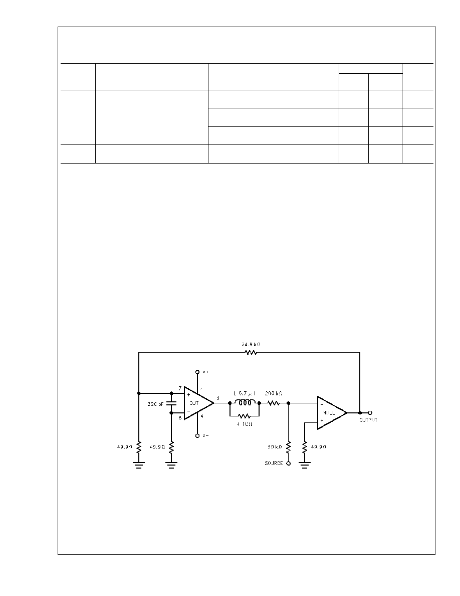
Test Circuit #1
(DC Electrical Test Circuit)
DS011449-3
LM3875
www.national.com
4
Test Circuit #2
(AC Electrical Test Circuit)
Single Supply Application Circuit
External Components Description
(
Figure 1 and Figure 2)
Components
Functional Description
1.
R
IN
Acts as a volume control by setting the voltage level allowed to the amplifier's input terminals.
2.
R
A
Provides DC voltage biasing for the single supply operation and bias current for the positive input terminal.
3.
C
A
Provides bias filtering.
4.
C
Provides AC coupling at the input and output of the amplifier for single supply operation.
5.
R
B
Prevents currents from entering the amplifier's non-inverting input which may be passed through to the load
upon power-down of the system due to the low input impedance of the circuitry when the under-voltage
circuitry is off. This phenomenon occurs when the supply voltages are below 1.5V.
6.
*
C
C
Reduces the gain (bandwidth of the amplifier) at high frequencies to avoid quasi-saturation oscillations of
the output transistor. The capacitor also suppresses external electromagnetic switching noise created from
fluorescent lamps.
7.
Ri
Inverting input resistance to provide AC Gain in conjunction with R
f1
.
DS011449-4
DS011449-5
*Optional components dependent upon specific design requirements. Refer to the External Components Description section for a component function
description.
FIGURE 2. Typical Single Supply Audio Amplifier Application Circuit
LM3875
www.national.com
5