 | –≠–ª–µ–∫—Ç—Ä–æ–Ω–Ω—ã–π –∫–æ–º–ø–æ–Ω–µ–Ω—Ç: LM388N-1 | –°–∫–∞—á–∞—Ç—å:  PDF PDF  ZIP ZIP |
TL H 7846
LM388
15W
Audio
Power
Amplifier
February 1995
LM388 1 5W Audio Power Amplifier
General Description
The LM388 is an audio amplifier designed for use in medium
power consumer applications The gain is internally set to
20 to keep external part count low but the addition of an
external resistor and capacitor between pins 2 and 6 will
increase the gain to any value up to 200
The inputs are ground referenced while the output is auto-
matically biased to one half the supply voltage
Features
Y
Minimum external parts
Y
Wide supply voltage range
Y
Excellent supply rejection
Y
Ground referenced input
Y
Self-centering output quiescent voltage
Y
Variable voltage gain
Y
Low distortion
Y
Fourteen pin dual-in-line package
Y
Low voltage operation 4V
Applications
Y
AM-FM radio amplifiers
Y
Portable tape player amplifiers
Y
Intercoms
Y
TV sound systems
Y
Lamp drivers
Y
Line drivers
Y
Ultrasonic drivers
Y
Small servo drivers
Y
Power converters
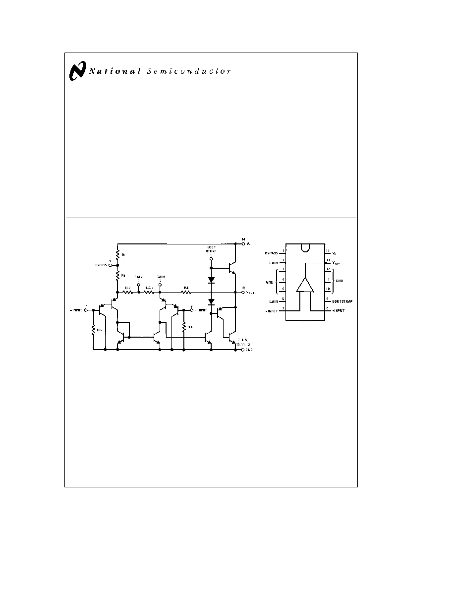
Equivalent Schematic and Connection Diagrams
TL H 7846 ≠ 1
Dual-In-Line Package
TL H 7846 ≠ 2
Top View
Order Number LM388N-1
See NS Package Number N14A
C1995 National Semiconductor Corporation
RRD-B30M115 Printed in U S A
Absolute Maximum Ratings
If Military Aerospace specified devices are required
please contact the National Semiconductor Sales
Office Distributors for availability and specifications
Supply Voltage
15V
Package Dissipation 14-Pin DIP (Note 1)
8 3W
Input Voltage
g
0 4V
Storage Temperature
b
65 C to
a
150 C
Operating Temperature
0 C to
a
70 C
Junction Temperature
150 C
Lead Temperature (Soldering 10 sec )
260 C
Thermal Resistance
i
JC
30 C W
i
JA
79 C W
Electrical Characteristics
T
A
e
25 C
(Figure 1)
Symbol
Parameter
Conditions
Min
Typ
Max
Units
V
S
Operating Supply Voltage
4
12
V
LM388
I
Q
Quiescent Current
V
IN
e
0
16
23
mA
LM388
V
S
e
12V
P
OUT
Output Power (Note 2)
R1
e
R2
e
180X THD
e
10%
LM388N-1
V
S
e
12V R
L
e
8X
1 5
2 2
W
V
S
e
6V R
L
e
4X
0 6
0 8
W
A
V
Voltage Gain
V
S
e
12V f
e
1 kHz
23
26
30
dB
10 mF from Pins 2 to 6
46
dB
BW
Bandwidth
V
S
e
12V Pins 2 and 6 Open
300
kHz
THD
Total Harmonic Distortion
V
S
e
12V R
L
e
8X P
OUT
e
500 mW
0 1
1
%
f
e
1 kHz Pins 2 and 6 Open
PSRR
Power Supply Rejection Ratio
V
S
e
12V f
e
1 kHz C
BYPASS
e
10 mF
50
dB
(Note 3)
Pins 2 and 6 Open Referred to Output
R
IN
Input Resistance
10
50
kX
I
BIAS
Input Bias Current
V
S
e
12V Pins 7 and 8 Open
250
nA
Note 1
Pins 3 4 5 10 11 12 at 25 C Derate at 15 C W above 25 C case
Note 2
The amplifier should be in high gain for full swing on higher supplies due to input voltage limitations
Note 3
If load and bypass capacitor are returned to V
S
(Figure 2) rather than ground (Figure 1) PSRR is typically 30 dB
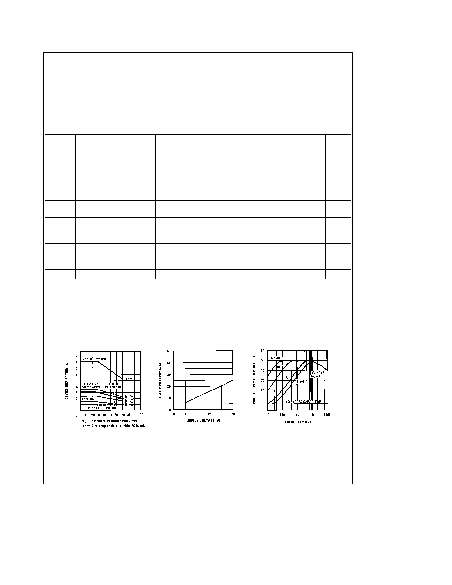
Typical Performance Characteristics
Ambient Temperature
Maximum Device Dissipation vs
Supply Voltage
Quiescent Supply Current vs
Frequency
(Referred to the Output) vs
Power Supply Rejection Ratio
TL H 7846 ≠ 5
2
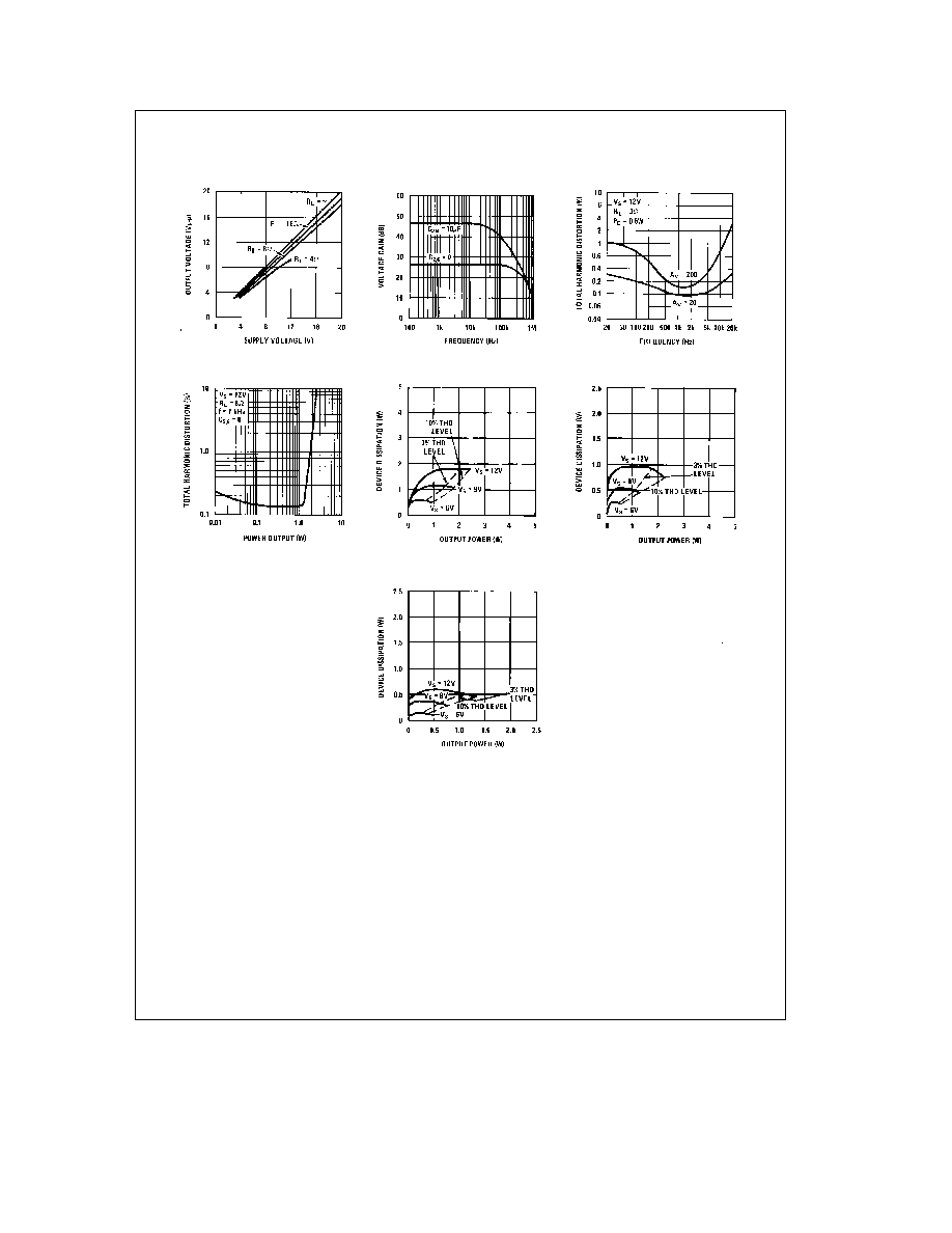
Typical Performance Characteristics
(Continued)
Swing vs Supply Voltage
Peak-to-Peak Output Voltage
Voltage Gain vs Frequency
Distortion vs Frequency
Distortion vs Output Power
Power
4X Load
Device Dissipation vs Output
Output Power
8X Load
Device Dissipation vs
Output Power
16X Load
Device Dissipation vs
TL H 7846 ≠ 6
Application Hints
GAIN CONTROL
To make the LM388 a more versatile amplifier two pins (2
and 6) are provided for gain control With pins 2 and 6 open
the 1 35 kX resistor sets the gain at 20 (26 dB) If a capaci-
tor is put from pins 2 to 6 bypassing the 1 35 kX resistor
the gain will go up to 200 (46 dB) If a resistor is placed in
series with the capacitor the gain can be set to any value
from 20 to 200 A low frequency pole in the gain response is
caused by the capacitor working against the external resis-
tor in series with the 150X internal resistor If the capacitor
is eliminated and a resistor connects pins 2 to 6 then the
output dc level may shift due to the additional dc gain Gain
control can also be done by capacitively coupling a resistor
(or FET) from pin 6 to ground as in
Figure 7
Additional external components can be placed in parallel
with the internal feedback resistors to tailor the gain and
frequency response for individual applications For example
we can compensate poor speaker bass response by fre-
quency shaping the feedback path This is done with a se-
ries RC from pin 6 to 13 (paralleling the internal 15 kX resis-
tor) For 6 dB effective bass boost R j 15 kX the lowest
value for good stable operation is R
e
10 kX if pin 2
3
Application Hints
(Continued)
is open If pins 2 and 6 are bypassed then R as low as 2 kX
can be used This restriction is because the amplifier is only
compensated for closed-loop gains greater than 9 V V
INPUT BIASING
The schematic shows that both inputs are biased to ground
with a 50 kX resistor The base current of the input transis-
tors is about 250 nA so the inputs are at about 12 5 mV
when left open If the dc source resistance driving the
LM388 is higher than 250 kX it will contribute very little
additional offset (about 2 5 mV at the input 50 mV at the
output) If the dc source resistance is less than 10 kX then
shorting the unused input to ground will keep the offset low
(about 2 5 mV at the input 50 mV at the output) For dc
source resistances between these values we can eliminate
excess offset by putting a resistor from the unused input to
ground equal in value to the dc source resistance Of
course all offset problems are eliminated if the input is ca-
pacitively coupled
When using the LM388 with higher gains (bypassing the
1 35 kX resistor between pins 2 and 6) it is necessary to
bypass the unused input preventing degradation of gain
and possible instabilities This is done with a 0 1 mF capaci-
tor or a short to ground depending on the dc source resist-
ance on the driven input
BOOTSTRAPPING
The base of the output transistor of the LM388 is brought
out to pin 9 for Bootstrapping The output stage of the am-
plifier during positive swing is shown in
Figure 3 with its
external circuitry
R1
a
R2 set the amount of base current available to the
output transistor The maximum output current divided by
beta is the value required for the current in R1 and R2
(R1
a
R2)
e
b
O
(V
S
2)
b
V
BE
I
O MAX
Good design values are V
BE
e
0 7V and b
O
e
100
Example 1 watt into 8X load with V
S
e
12V
I
O MAX
e
0
2 P
O
R
L
e
500 mA
(R1
a
R2)
e
100
(12 2)
b
0 7
0 5
J
e
1060X
To keep the current in R2 constant during positive swing
capacitor C
B
is added As the output swings positive C
B
lifts
R1 and R2 above the supply maintaining a constant voltage
across R2 To minimize the value of C
B
R1
e
R2 The pole
due to C
B
and R1 and R2 is usually set equal to the pole
due to the output coupling capacitor and the load This
gives
C
B
j
4C
c
b
O
j
C
c
25
Example for 100 Hz pole and R
L
e
8X C
c
e
200 mF and
C
B
e
8 mF if R1 is made a diode and R2 increased to give
the same current C
B
can be decreased by about a factor of
4 as in
Figure 4
For reduced component count the load can replace R1 The
value of (R1
a
R2) is the same so R2 is increased Now C
B
is both the coupling and the bootstrapping capacitor (see
Figure 2 )
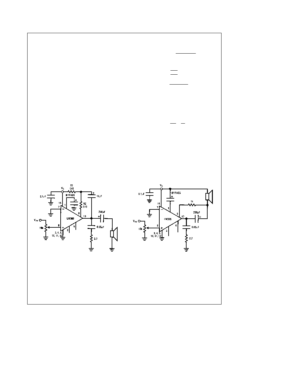
Typical Applications
TL H 7846 ≠ 3
FIGURE 1 Load Returned to Ground
(Amplifier with Gain
e
20)
TL H 7846 ≠ 4
FIGURE 2 Load Returned to V
S
(Amplifier with Gain
e
20)
4
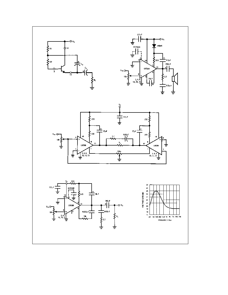
Typical Applications
(Continued)
TL H 7846 ≠ 7
FIGURE 3
TL H 7846 ≠ 8
FIGURE 4 Ampifier with Gain
e
200 and Minimum C
B
TL H 7846 ≠ 9
V
S
e
6V
R
L
e
4X
P
O
e
1 0W
V
S
e
12V
R
L
e
8X
P
O
e
4W
FIGURE 5 Bridge Amp
TL H 7846 ≠ 10
FIGURE 6a Amplifier with Bass Boost
TL H 7846 ≠ 11
FIGURE 6b Frequency Response
with Bass Boost
5