 | –≠–ª–µ–∫—Ç—Ä–æ–Ω–Ω—ã–π –∫–æ–º–ø–æ–Ω–µ–Ω—Ç: LM389N | –°–∫–∞—á–∞—Ç—å:  PDF PDF  ZIP ZIP |
TL H 7847
LM389
Low
Voltage
Audio
Power
Amplifier
with
NPN
Transistor
Array
December 1994
LM389 Low Voltage Audio Power Amplifier
with NPN Transistor Array
General Description
The LM389 is an array of three NPN transistors on the same
substrate with an audio power amplifier similar to the
LM386
The amplifier inputs are ground referenced while the output
is automatically biased to one half the supply voltage The
gain is internally set at 20 to minimize external parts but the
addition of an external resistor and capacitor between pins
4 and 12 will increase the gain to any value up to 200
The three transistors have high gain and excellent matching
characteristics They are well suited to a wide variety of ap-
plications in DC through VHF systems
Features
Amplifier
Y
Battery operation
Y
Minimum external parts
Y
Wide supply voltage range
Y
Low quiescent current drain
Y
Voltage gains from 20 to 200
Y
Ground referenced input
Y
Self-centering output quiescent voltage
Y
Low distortion
Transistors
Y
Operation from 1 mA to 25 mA
Y
Frequency range from DC to 100 MHz
Y
Excellent matching
Applications
Y
AM-FM radios
Y
Portable tape recorders
Y
Intercoms
Y
Toys and games
Y
Walkie-talkies
Y
Portable phonographs
Y
Power converters
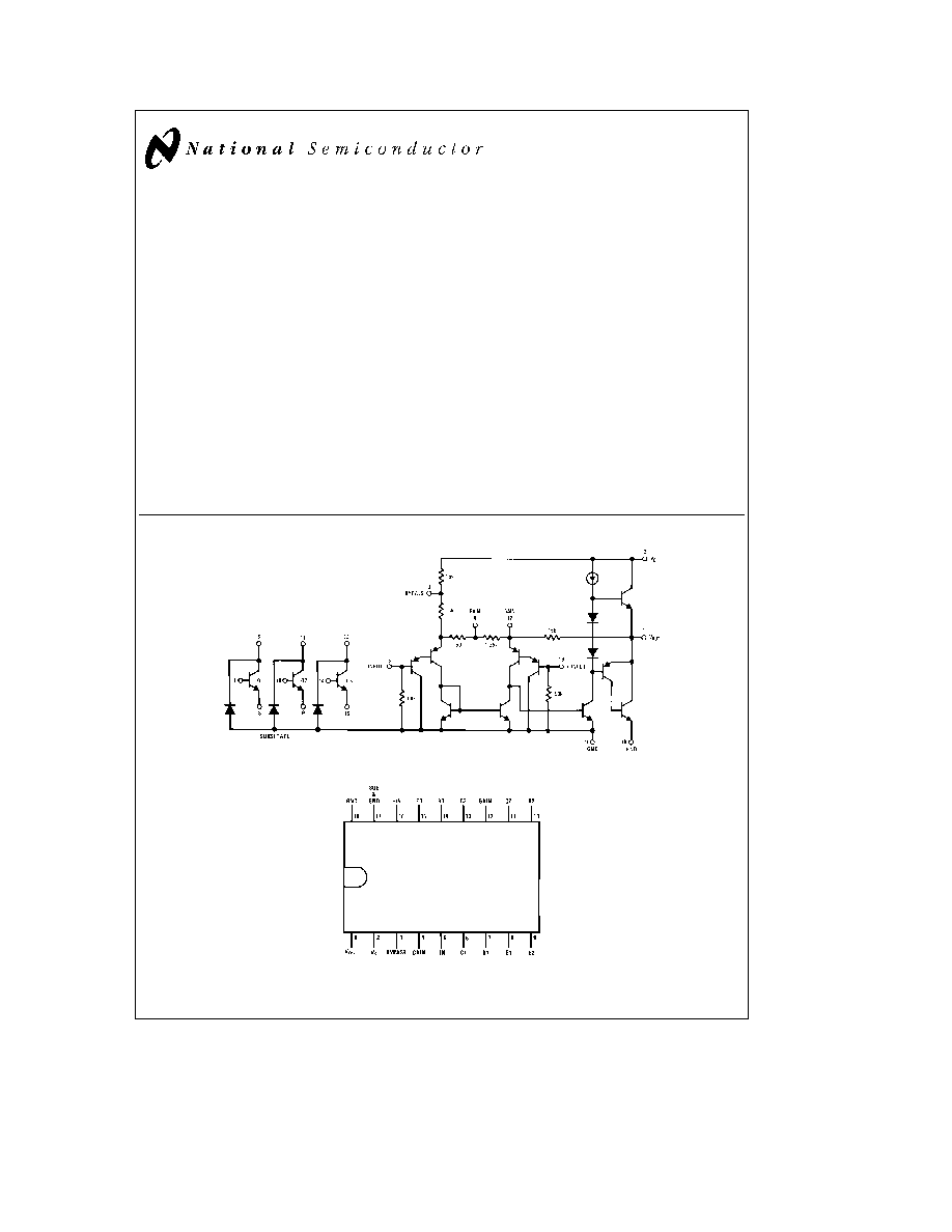
Equivalent Schematic and Connection Diagrams
TL H 7847 ≠ 1
Dual-In-Line Package
TL H 7847 ≠ 2
Order Number LM389N
See NS Package Number N18A
C1995 National Semiconductor Corporation
RRD-B30M115 Printed in U S A
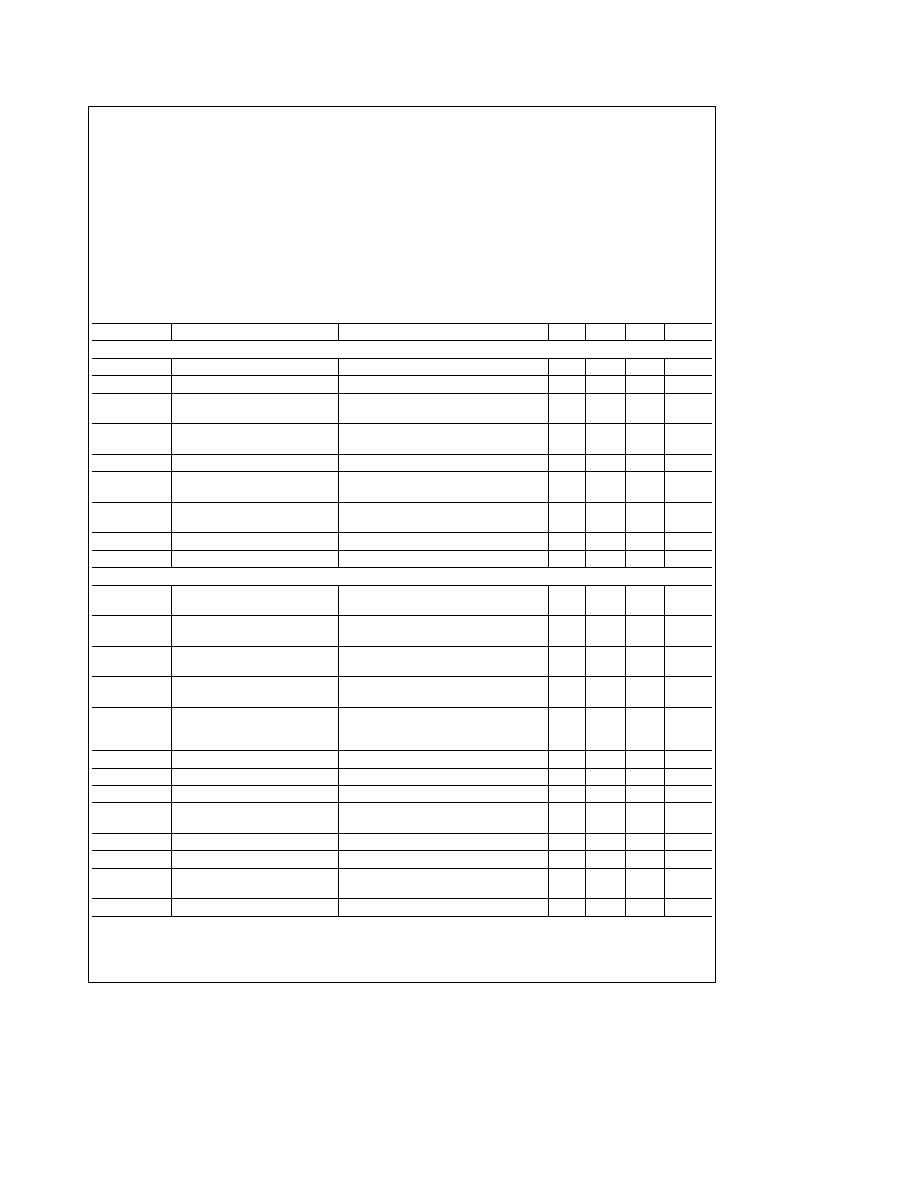
Absolute Maximum Ratings
If Military Aerospace specified devices are required
please contact the National Semiconductor Sales
Office Distributors for availability and specifications
Supply Voltage
15V
Package Dissipation (Note 1)
1 89W
Input Voltage
g
0 4V
Storage Temperature
b
65 C to
a
150 C
Operating Temperature
0 C to
a
70 C
Junction Temperature
150 C
Lead Temperature (Soldering 10 sec )
260 C
Collector to Emitter Voltage V
CEO
12V
Collector to Base Voltage V
CBO
15V
Collector to Substrate Voltage V
CIO
(Note 2)
15V
Collector Current I
C
25 mA
Emitter Current I
E
25 mA
Base Current I
B
5 mA
Power Dissipation (Each Transistor) T
A
s
a
70 C
150 mW
Thermal Resistance
i
JC
24 C W
i
JA
70 C W
Electrical Characteristics
T
A
e
25 C
Symbol
Parameter
Conditions
Min
Typ
Max
Units
AMPLIFIER
V
S
Operating Supply Voltage
4
12
V
I
Q
Quiescent Current
V
S
e
6V V
IN
e
0V
6
12
mA
P
OUT
Output Power (Note 3)
THD
e
10%
V
S
e
6V R
L
e
8X
250
325
mW
V
S
e
9V R
L
e
16X
500
mW
A
V
Voltage Gain
V
S
e
6V f
e
1 kHz
23
26
30
dB
10 mF from Pins 4 to 12
46
dB
BW
Bandwidth
V
S
e
6V Pins 4 and 12 Open
250
kHz
THD
Total Harmonic Distortion
V
S
e
6V R
L
e
8X P
OUT
e
125 mW
0 2
3 0
%
f
e
1 kHz Pins 4 and 12 Open
PSRR
Power Supply Rejection Ratio
V
S
e
6V f
e
1 kHz C
BYPASS
e
10 mF
30
50
dB
Pins 4 and 12 Open Referred to Output
R
IN
Input Resistance
10
50
kX
I
BIAS
Input Bias Current
V
S
e
6V Pins 5 and 16 Open
250
nA
TRANSISTORS
V
CEO
Collector to Emitter
I
C
e
1 mA I
B
e
0
12
20
V
Breakdown Voltage
V
CBO
Collector to Base
I
C
e
10 mA I
E
e
0
15
40
V
Breakdown Voltage
V
CIO
Collector to Substrate
I
C
e
10 mA I
E
e
I
B
e
0
15
40
V
Breakdown Voltage
V
EBO
Emitter to Base
I
E
e
10 mA I
C
e
0
6 4
7 1
7 8
V
Breakdown Voltage
H
FE
Static Forward Current
I
C
e
10 mA
100
Transfer Ratio (Static Beta)
I
C
e
1 mA
100
275
I
C
e
10 mA
275
h
oe
Open-Circuit Output Admittance
I
C
e
1 mA V
CE
e
5V f
e
1 0 kHz
20
m
mho
V
BE
Base to Emitter Voltage
I
E
e
1 mA
0 7
0 85
V
l
V
BE1
≠ V
BE2
l
Base to Emitter Voltage Offset
I
E
e
1 mA
1
5
mV
V
CESAT
Collector to Emitter
I
C
e
10 mA I
B
e
1 mA
0 15
0 5
V
Saturation Voltage
C
EB
Emitter to Base Capacitance
V
EB
e
3V
1 5
pF
C
CB
Collector to Base Capacitance
V
CB
e
3V
2
pF
C
CI
Collector to Substrate
V
CI
e
3V
3 5
pF
Capacitance
h
fe
High Frequency Current Gain
I
C
e
10 mA V
CE
e
5V f
e
100 MHz
1 5
5 5
Note 1
For operation in ambient temperatures above 25 C the device must be derated based on a 150 C maximum junction temperature and a thermal resistance
of 66 C W junction to ambient
Note 2
The collector of each transistor is isolated from the substrate by an integral diode Therefore the collector voltage should remain positive with respect to
pin 17 at all times
Note 3
If oscillation exists under some load conditions add 2 7X and 0 05 mF series network from pin 1 to ground
2
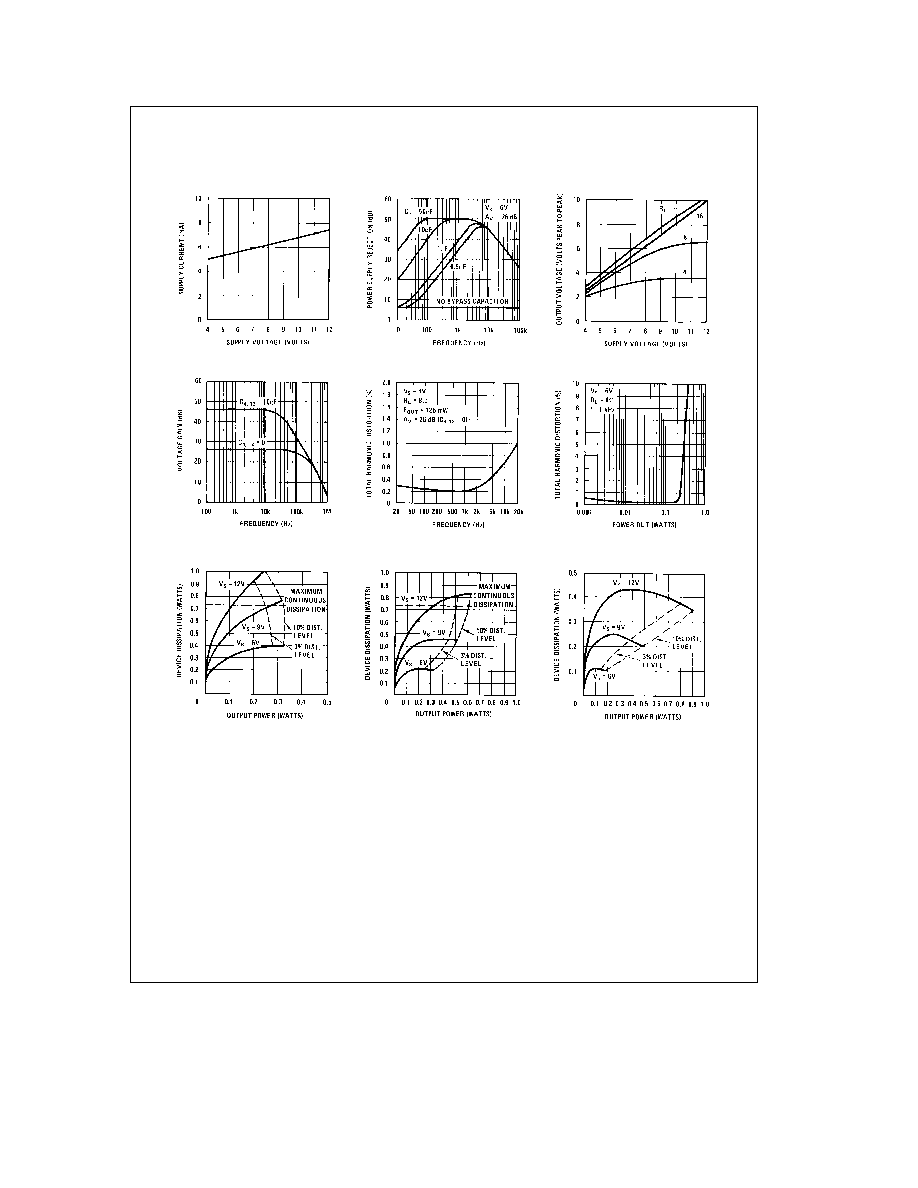
Typical Amplifier Performance Characteristics
vs Supply Voltage
Quiescent Supply Current
vs Frequency
(Referred to the Output)
Power Supply Rejection Ratio
Swing vs Supply Voltage
Peak-to-Peak Output Voltage
Voltage Gain vs Frequency
Distortion vs Frequency
Distortion vs Output Power
Power
4X Load
Device Dissipation vs Output
Power
8X Load
Device Dissipation vs Output
Power
16X Load
Device Dissipation vs Output
TL H 7847 ≠ 3
3
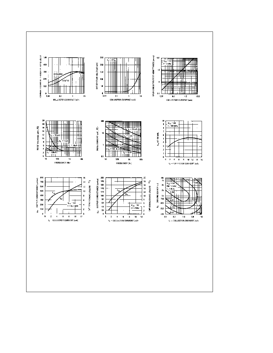
Typical Transistor Performance Characteristics
vs Collector Current
Forward Current Transfer Ratio
Collector Current
Saturation Voltage vs
vs Collector Current
Open Circuit Output Admittance
TL H 7847 ≠ 4
Noise Voltage vs Frequency
Noise Current vs Frequency
vs Collector Current
High Frequency Current Gain
Current
g
oe
and C
oe
vs Collector
Current
g
oe
and C
oe
vs Collector
Figure
Contours of Constant Noise
TL H 7847 ≠ 5
4
Application Hints
Gain Control
To make the LM389 a more versatile amplifier two pins (4
and 12) are provided for gain control With pins 4 and 12
open the 1 35 kX resistor sets the gain at 20 (26 dB) If a
capacitor is put from pin 4 to 12 bypassing the 1 35 kX
resistor the gain will go up to 200 (46 dB) If a resistor is
placed in series with the capacitor the gain can be set to
any value from 20 to 200 A low frequency pole in the gain
response is caused by the capacitor working against the
external resistor in series with the 150X internal resistor If
the capacitor is eliminated and a resistor connects pin 4 to
12 then the output dc level may shift due to the additional
dc gain Gain control can also be done by capacitively cou-
pling a resistor (or FET) from pin 12 to ground
Additional external components can be placed in parallel
with the internal feedback resistors to tailor the gain and
frequency response for individual applications For example
we can compensate poor speaker bass response by fre-
quency shaping the feedback path This is done with a se-
ries RC from pin 1 to 12 (paralleling the internal 15 kX resis-
tor) For 6 dB effective bass boost R j 15 kX the lowest
value for good stable operation is R
e
10 kX if pin 4 is
open If pins 4 and 12 are bypassed then R as low as 2 kX
can be used This restriction is because the amplifier is only
compensated for closed-loop gains greater than 9V V
Input Biasing
The schematic shows that both inputs are biased to ground
with a 50 kX resistor The base current of the input transis-
tors is about 250 nA so the inputs are at about 12 5 mV
when left open If the dc source resistance driving the
LM389 is higher than 250 kX it will contribute very little
additional offset (about 2 5 mV at the input 50 mV at the
output) If the dc source resistance is less than 10 kX then
shorting the unused input to ground will keep the offset low
(about 2 5 mV at the input 50 mV at the output) For dc
source resistances between these values we can eliminate
excess offset by putting a resistor from the unused input to
ground equal in value to the dc source resistance Of
course all offset problems are eliminated if the input is ca-
pacitively coupled
When using the LM389 with higher gains (bypassing the
1 35 kX resistor between pins 4 and 12) it is necessary to
bypass the unused input preventing degradation of gain
and possible instabilities This is done with a 0 1 mF capaci-
tor or a short to ground depending on the dc source resist-
ance of the driven input
Supplies and Grounds
The LM389 has excellent supply rejection and does not re-
quire a well regulated supply However to eliminate possi-
ble high frequency stability problems the supply should be
decoupled to ground with a 0 1 mF capacitor The high cur-
rent ground of the output transistor pin 18 is brought out
separately from small signal ground pin 17 If the two
ground leads are returned separately to supply then the par-
asitic resistance in the power ground lead will not cause
stability problems The parasitic resistance in the signal
ground can cause stability problems and it should be mini-
mized Care should also be taken to insure that the power
dissipation does not exceed the maximum dissipation of the
package for a given temperature There are two ways to
mute the LM389 amplifier Shorting pin 3 to the supply volt-
age or shorting pin 12 to ground will turn the amplifier off
without affecting the input signal
Transistors
The three transistors on the LM389 are general purpose
devices that can be used the same as other small signal
transistors As long as the currents and voltages are kept
within the absolute maximum limitations and the collectors
are never at a negative potential with respect to pin 17
there is no limit on the way they can be used
For example the emitter-base breakdown voltage of 7 1V
can be used as a zener diode at currents from 1 mA to
5 mA These transistors make good LED driver devices
V
SAT
is only 150 mV when sinking 10 mA
In the linear region these transistors have been used in AM
and FM radios tape recorders phonographs and many oth-
er applications Using the characteristic curves on noise
voltage and noise current the level of the collector current
can be set to optimize noise performance for a given source
impedance Some of the circuits that have been built are
shown in
Figures 1 ≠ 7 This is by no means a complete list
of applications since that is limited only by the designers
imagination
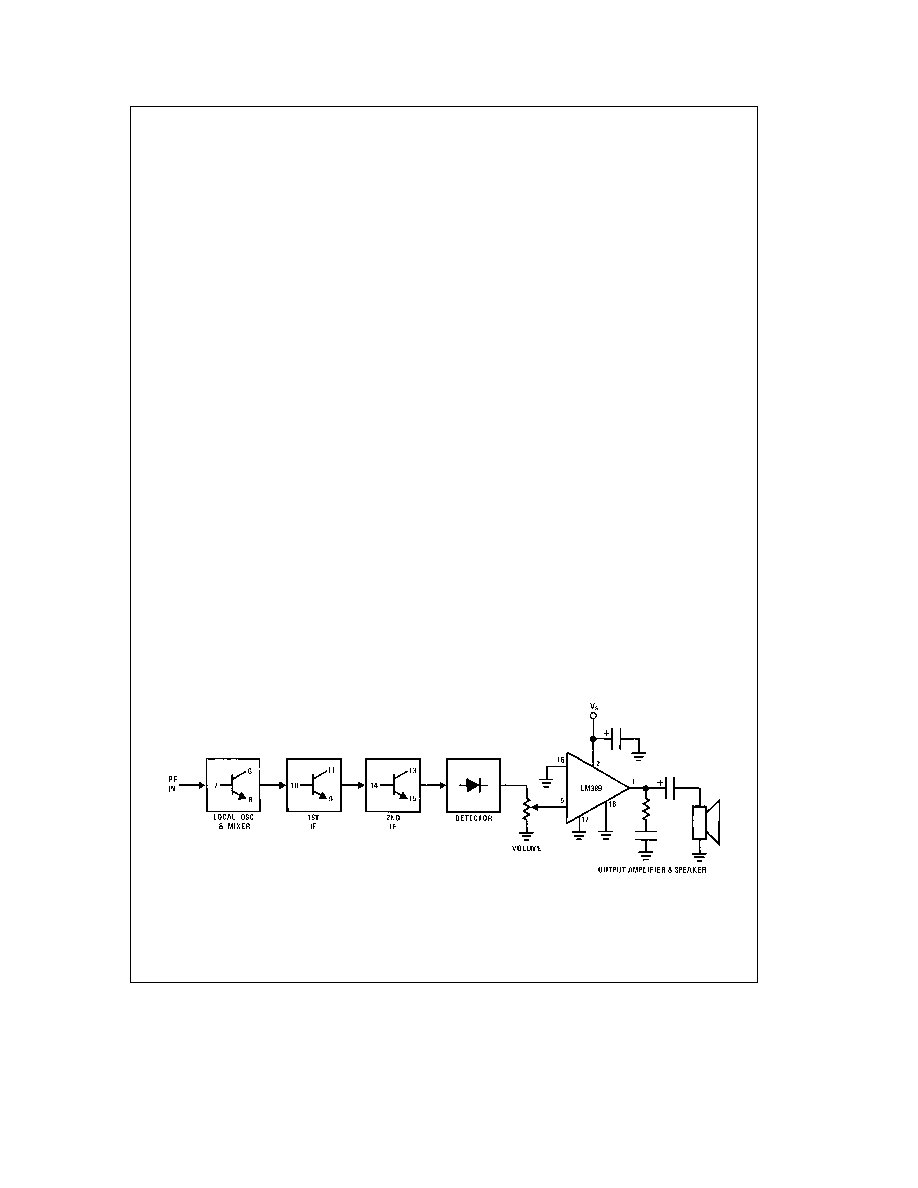
TL H 7847 ≠ 6
FIGURE 1 AM Radio
5