 | –≠–ª–µ–∫—Ç—Ä–æ–Ω–Ω—ã–π –∫–æ–º–ø–æ–Ω–µ–Ω—Ç: LM3916 | –°–∫–∞—á–∞—Ç—å:  PDF PDF  ZIP ZIP |

LM3916
Dot/Bar Display Driver
General Description
The LM3916 is a monolithic integrated circuit that senses
analog voltage levels and drives ten LEDs, LCDs or vacuum
fluorescent displays, providing an electronic version of the
popular VU meter. One pin changes the display from a bar
graph to a moving dot display. LED current drive is regulated
and programmable, eliminating the need for current limiting
resistors. The whole display system can operate from a
single supply as low as 3V or as high as 25V.
The IC contains an adjustable voltage reference and an ac-
curate ten-step voltage divider. The high-impedance input
buffer accepts signals down to ground and up to within 1.5V
of the positive supply. Further, it needs no protection against
inputs of
±
35V. The input buffer drives 10 individual com-
parators referenced to the precision divider. Accuracy is typi-
cally better than 0.2 dB.
Audio applications include average or peak level indicators,
and power meters. Replacing conventional meters with an
LED bar graph results in a faster responding, more rugged
display with high visibility that retains the ease of interpreta-
tion of an analog display.
The LM3916 is extremely easy to apply. A 1.2V full-scale
meter requires only one resistor in addition to the ten LEDs.
One more resistor programs the full-scale anywhere from
1.2V to 12V independent of supply voltage. LED brightness
is easily controlled with a single pot.
The LM3916 is very versatile. The outputs can drive LCDs,
vacuum fluorescents and incandescent bulbs as well as
LEDs of any color. Multiple devices can be cascaded for a
dot or bar mode display for increased range and/or resolu-
tion. Useful in other applications are the linear LM3914 and
the logarithmic LM3915.
Features
n
Fast responding electronic VU meter
n
Drivers LEDs, LCDs, or vacuum fluorescents
n
Bar or dot display mode externally selectable by user
n
Expandable to displays of 70 dB
n
Internal voltage reference from 1.2V to 12V
n
Operates with single supply of 3V to 25V
n
Inputs operate down to ground
n
Output current programmable from 1 mA to 30 mA
n
Input withstands
±
35V without damage or false outputs
n
Outputs are current regulated, open collectors
n
Directly drives TTL or CMOS
n
The internal 10-step divider is floating and can be
referenced to a wide range of voltages
The LM3916 is rated for operation from 0∞C to +70∞C. The
LM3916N-1 is available in an 18-lead molded DIP package.
January 2000
LM3916
Dot/Bar
Display
Driver
© 2000 National Semiconductor Corporation
DS007971
www.national.com
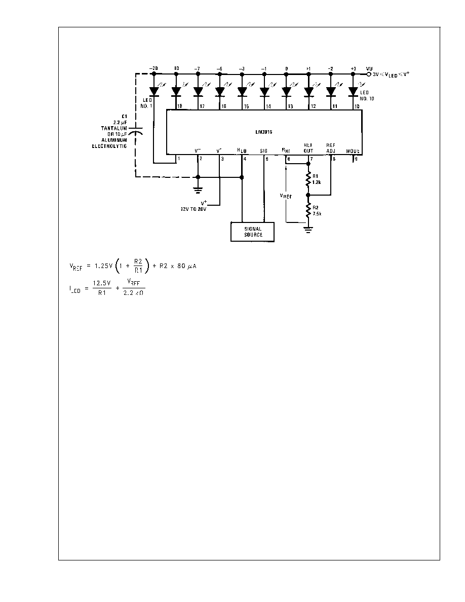
Typical Applications
0V to 10V VU Meter
DS007971-1
Notes: Capacitor C1 is required if leads to the LED supply are 6" or longer.
Circuit as shown is wired for dot mode. For bar mode, connect pin 9 to pin 3. V
LED
must be kept below 7V or dropping resistor should be used to limit IC power
dissipation.
LM3916
www.national.com
2
Absolute Maximum Ratings
(Note 1)
If Military/Aerospace specified devices are required,
please contact the National Semiconductor Sales Office/
Distributors for availability and specifications.
Power Dissipation (Note 6)
Molded DIP (N)
1365 mW
Supply Voltage
25V
Voltage on Output Drivers
25V
Input Signal Overvoltage (Note 4)
±
35V
Divider Voltage
-100 mV to V
+
Reference Load Current
10 mA
Storage Temperature Range
-55∞C to +150∞C
Lead Temperature
(Soldering, 10 seconds)
260∞C
Electrical Characteristics
(Notes 2, 4)
Parameter
Conditions (Note 2)
Min
Typ
Max
Units
COMPARATORS
Offset Voltage, Buffer and First Comparator
0V
V
RLO
= V
RHI
12V,
I
LED
= 1 mA
3
10
mV
Offset Voltage, Buffer and Any Other Comparator
0V
V
RLO
= V
RHI
12V,
I
LED
= 1 mA
3
15
mV
Gain (
I
LED
/
V
IN
)
I
(REF)
= 2 mA, I
LED
= 10 mA
3
8
mA/mV
Input Bias Current (at Pin 5)
0V
V
IN
(V
+
-1.5V)
25
100
nA
Input Signal Overvoltage
No Change in Display
-35
35
V
VOLTAGE DIVIDER
Divider Resistance
Total, Pin 6 to 4
8
12
17
k
Relative Accuracy (Input Change
Between Any Two Threshold Points)
(Note 3)
-1 dB
V
IN
3 dB
-7 dB
V
IN
-1 dB
-10 dB
V
IN
-7 dB
0.75
1.5
2.5
1.0
2.0
3.0
1.25
2.5
2.5
dB
dB
dB
Absolute Accuracy
(Note 3)
V
IN
= 2, 1, 0, -1 dB
V
IN
= -3, -5 dB
V
IN
= -7, -10, -20 dB
-0.25
-0.5
-1
+0.25
+0.5
+1
dB
dB
dB
VOLTAGE REFERENCE
Output Voltage
0.1 mA
I
L(REF)
4 mA,
V
+
= V
LED
= 5Vg
1.2
1.28
1.34
V
Line Regulation
3V
V
+
18V
0.01
0.03
%/V
Load Regulation
0.1 mA
I
L(REF)
4 mA,
V
+
= V
LED
= 5V
0.4
2
%
Output Voltage Change with Temperature
0∞C
T
A
+70∞C, I
L(REF)
= 1 mA,
V
+
= V
LED
= 5V
1
%
Adjust Pin Current
75
120
µA
OUTPUT DRIVERS
LED Current
V
+
= V
LED
= 5V, I
L(REF)
= 1 mA
7
10
13
mA
LED Current Difference (Between Largest and
Smallest LED Currents)
V
LED
= 5V, I
LED
= 2 mA
V
LED
= 5V, I
LED
= 20 mA
0.12
1.2
0.4
3
mA
mA
LED Current Regulation
2V
V
LED
17V
I
LED
2 mA
I
LED
= 20 mA
0.1
1
0.25
3
mA
mA
Dropout Voltage
I
LED(ON)
= 20 mA
@
V
LED
= 5V,
I
LED
= 2 mA
1.5
V
Saturation Voltage
I
LED
= 2.0 mA, I
L(REF)
= 0.4 mA
0.15
0.4
V
Output Leakage, Each Collector
Bar Mode (Note 5)
0.1
100
µA
Output Leakage
Dot Mode (Note 5)
Pins 10≠18
0.1
100
µA
Pin 1
60
150
450
µA
LM3916
www.national.com
3
Electrical Characteristics
(Notes 2, 4) (Continued)
Parameter
Conditions (Note 2)
Min
Typ
Max
Units
SUPPLY CURRENT
Standby Supply Current
(All Outputs Off)
V
+
= + 5V, I
L(REF)
= 0.2 mA
V
+
= + 20V, I
L(REF)
= 1.0 mA
2.4
6.1
4.2
9.2
mA
mA
Note 1: Absolute Maximum Ratings indicate limits beyond which damage to the device may occur. Operating ratings indicate conditions for which the device is func-
tional, but do not guarantee specific performance limits. Electrical Characteristics state DC and AC electrical specifications under particular test conditions which guar-
antee specific performance limits. This assumes that the device is within the Operating Ratings. Specifications are not guaranteed for parameters where no limit is
given, however, the typical value is a good indication of device performance.
Note 2: Unless otherwise stated, all specifications apply with the following conditions:
3 V
DC
V
+
20 V
DC
-0.015V
V
RLO
12 V
DC
T
A
= 25∞C, I
L(REF)
= 0.2 mA, pin 9 connected to pin 3 (bar mode).
3 V
DC
V
LED
V
+
V
REF
, V
RHI
, V
RLO
(V
+
- 1.5V)
For higher power dissipations, pulse testing is used.
-0.015V
V
RHI
12 V
DC
0V
V
IN
V
+
- 1.5V
Note 3: Accuracy is measured referred to +3 dB = +10.000 V
DC
at pin 5, with +10.000 V
DC
at pin 6, and 0.000 V
DC
at pin 4. At lower full-scale voltages, buffer and
comparator offset voltage may add significant error. See table for threshold voltages.
Note 4: Pin 5 input current must be limited to
±
3 mA. The addition of a 39k resistor in series with pin 5 allows
±
100V signals without damage.
Note 5: Bar mode results when pin 9 is within 20 mV of V
+
. Dot mode results when pin 9 is pulled at least 200 mV below V
+
. LED #10 (pin 10 output current) is dis-
abled if pin 9 is pulled 0.9V or more below V
LED
.
Note 6: The maximum junction temperature of the LM3916 is 100∞C. Devices must be derated for operation at elevated temperatures. Junction to ambient thermal
resistance is 55∞C/W for the molded DIP (N package).
LM3916 Threshold Voltage
(Note 3)
dB
Volts
dB
Volts
Min
Typ
Max
Min
Typ
Max
3
9.985
10.000
10.015
-3
±
1
/
2
4.732
5.012
5.309
2
±
1
/
4
8.660
8.913
9.173
-5
±
1
/
2
3.548
3.981
4.467
1
±
1
/
4
7.718
7.943
8.175
-7
±
1
2.818
3.162
3.548
0
±
1
/
4
6.879
7.079
7.286
-10
±
1
1.995
2.239
2.512
-1
±
1
/
2
5.957
6.310
6.683
-20
±
1
0.631
0.708
0.794
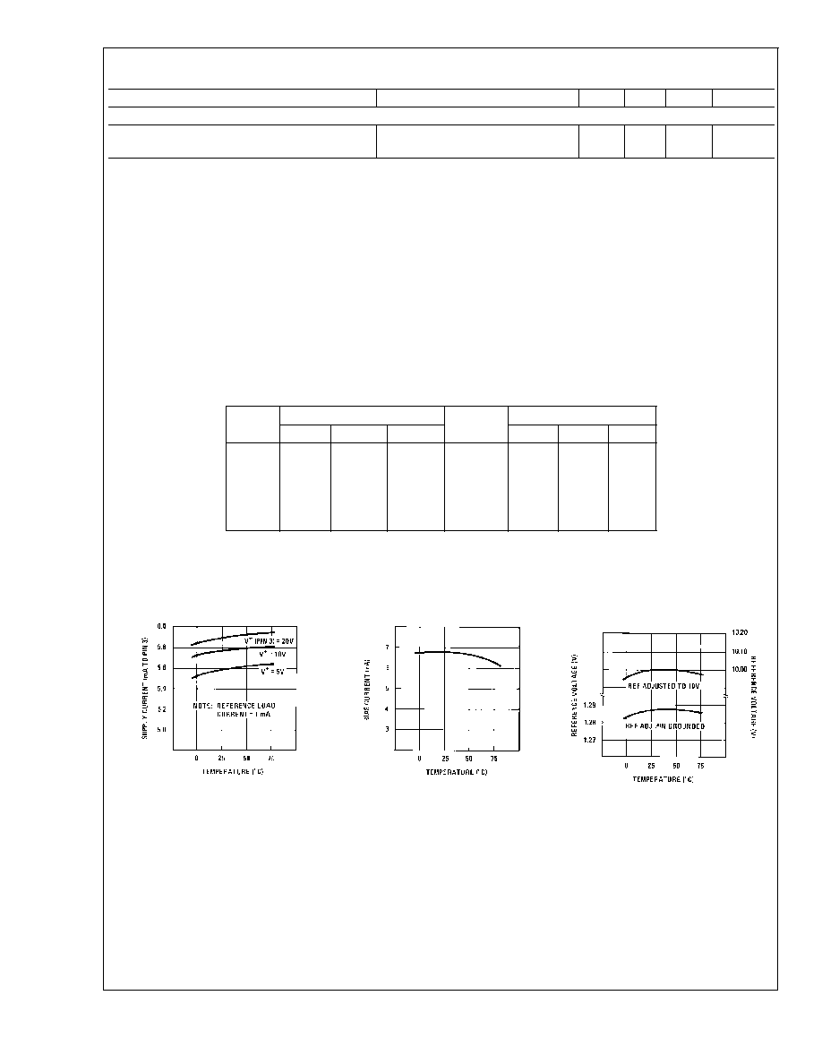
Typical Performance Characteristics
Supply Current vs
Temperature
DS007971-35
Operating Input Bias
Current vs Temperature
DS007971-36
Reference Voltage vs
Temperature
DS007971-37
LM3916
www.national.com
4
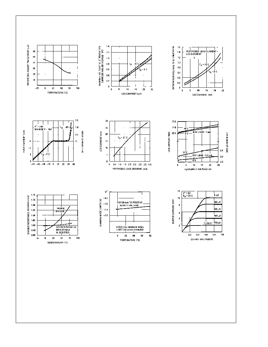
Typical Performance Characteristics
(Continued)
Reference Adjust Pin
Current vs Temperature
DS007971-38
LED Current-Regulation
Dropout
DS007971-39
LED Driver Saturation
Voltage
DS007971-40
Input Current Beyond
Signal Range (Pin 5)
DS007971-41
LED Current vs
Referenced Loading
DS007971-42
LED Driver Current
Regulation
DS007971-43
Total Divider Resistance
vs Temperature
DS007971-44
Common-Mode Limits
DS007971-45
Output Characteristics
DS007971-46
LM3916
www.national.com
5