LM3940
1A Low Dropout Regulator for 5V to 3.3V Conversion
General Description
The LM3940 is a 1A low dropout regulator designed to
provide 3.3V from a 5V supply.
The LM3940 is ideally suited for systems which contain both
5V and 3.3V logic, with prime power provided from a 5V bus.
Because the LM3940 is a true low dropout regulator, it can
hold its 3.3V output in regulation with input voltages as low
as 4.5V.
The T0-220 package of the LM3940 means that in most
applications the full 1A of load current can be delivered
without using an additional heatsink.
The surface mount TO-263 package uses minimum board
space, and gives excellent power dissipation capability when
soldered to a copper plane on the PC board.
Features
n
Output voltage specified over temperature
n
Excellent load regulation
n
Guaranteed 1A output current
n
Requires only one external component
n
Built-in protection against excess temperature
n
Short circuit protected
Applications
n
Laptop/Desktop Computers
n
Logic Systems
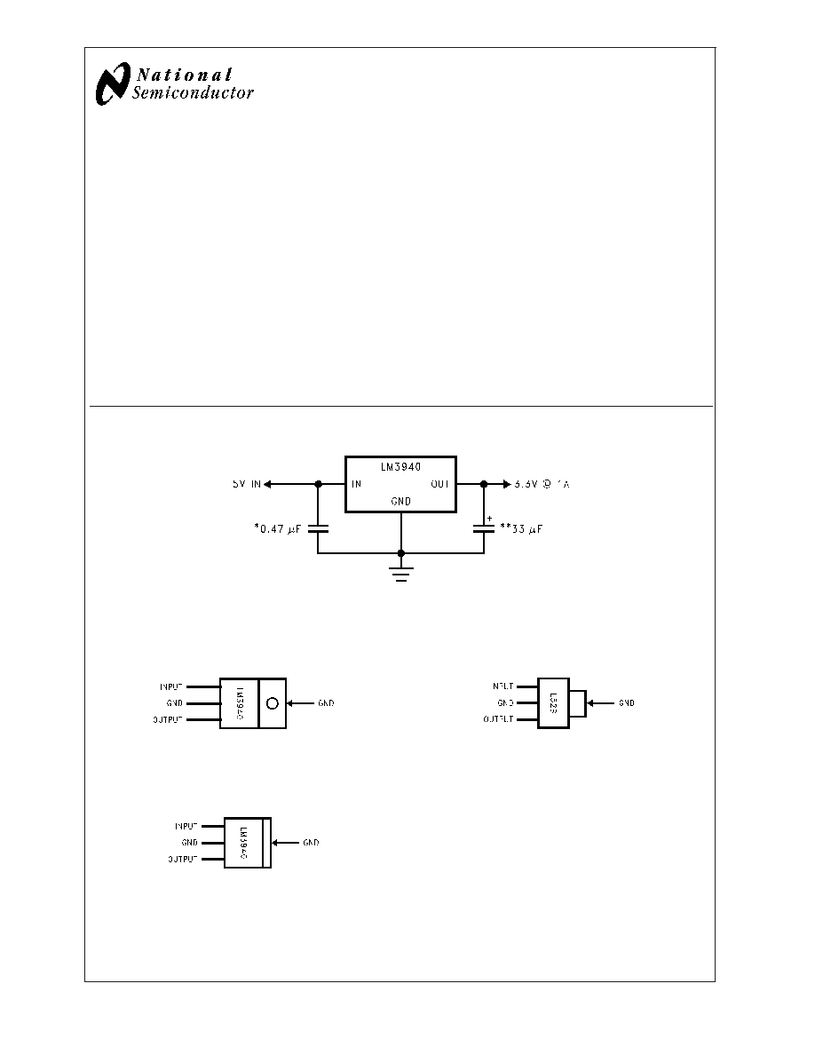
Typical Application
01208001
*Required if regulator is located more than 1" from the power supply filter capacitor or if battery power is used.
**See Application Hints.
Connection Diagram/Ordering Information
01208002
3-Lead TO-220 Package
(Front View)
Order Part Number LM3940IT-3.3
NSC Drawing Number TO3B
01208003
3-Lead TO-263 Package
(Front View)
Order Part Number LM3940IS-3.3
NSC Drawing Number TS3B
01208010
3-Lead SOT-223
(Front View)
Order Part Number LM3940IMP-3.3
Package Marked L52B
NSC Drawing Number MP04A
January 2003
LM3940
1A
Low
Dropout
Regulator
for
5V
to
3.3V
Conversion
� 2003 National Semiconductor Corporation
DS012080
www.national.com

Connection Diagram/Ordering
Information
(Continued)
01208027
16-Lead Ceramic Dual-in-Line Package
(Top View)
Order Part Number LM3940J-3.3-QML
5962-9688401QEA
NSC Drawing Number J16A
01208028
16-Lead Ceramic Surface-Mount Package
(Top View)
Order Part Number LM3940WG-3.3-QML
5962-9688401QXA
NSC Drawing Number WG16A
8-Lead LLP
01208030
Pin 2 and pin 7 are fused to center DAP
Pin 5 and 6 need to be tied together on PCB board
(Top View)
Order Part Number LM3940LD-3.3
NSC Drawing Number LDC08A
LM3940
www.national.com
2
Absolute Maximum Ratings
(Note 1)
If Military/Aerospace specified devices are required,
please contact the National Semiconductor Sales Office/
Distributors for availability and specifications.
Storage Temperature Range
-65�C to +150�C
Operating Junction Temperature Range -40�C to +125�C
Lead Temperature (Soldering, 5 seconds)
260�C
Power Dissipation (Note 2)
Internally Limited
Input Supply Voltage
7.5V
ESD Rating (Note 3)
2 kV
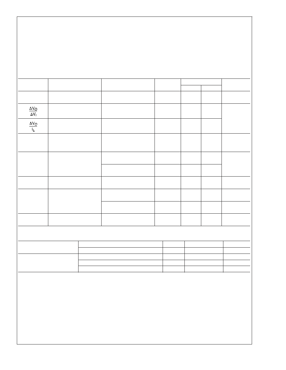
Electrical Characteristics
Limits in standard typeface are for T
J
= 25�C, and limits in boldface type apply over the full operating temperature range. Un-
less otherwise specified: V
IN
= 5V, I
L
= 1A, C
OUT
= 33 �F.
Symbol
Parameter
Conditions
Typical
LM3940 (Note 4)
Units
min
max
V
O
Output Voltage
5 mA
I
L
1A
3.3
3.20
3.40
V
3.13
3.47
Line Regulation
I
L
= 5 mA
20
40
mV
4.5V
V
O
5.5V
Load Regulation
50 mA
I
L
1A
35
50
80
Z
O
Output Impedance
I
L
(DC) = 100 mA
I
L
(AC) = 20 mA (rms)
35
m
f = 120 Hz
I
Q
Quiescent Current
4.5V
V
IN
5.5V
10
15
mA
I
L
= 5 mA
20
V
IN
= 5V
110
200
I
L
= 1A
250
e
n
Output Noise Voltage
BW = 10 Hz�100 kHz
150
�V (rms)
I
L
= 5 mA
V
O
- V
IN
Dropout Voltage
I
L
= 1A
0.5
0.8
V
(Note 5)
1.0
I
L
= 100 mA
110
150
mV
200
I
L
(SC)
Short Circuit Current
R
L
= 0
1.7
1.2
A
Thermal Performance
Thermal Resistance
Junction-to-Case
3-Lead TO-220
4
�C/W
3-Lead TO-263
4
�C/W
Thermal Resistance
Junction-to-Ambient
3-Lead TO-220
60
�C/W
3-Lead TO-263
80
�C/W
8-Lead LLP (Note 2)
35
�C/W
Note 1: Absolute maximum ratings indicate limits beyond which damage to the component may occur. Electrical specifications do not apply when operating the
device outside of its rated operating conditions.
Note 2: The maximum allowable power dissipation is a function of the maximum junction temperature, T
J
, the junction-to-ambient thermal resistance,
JA
, and the
ambient temperature, T
A
. Exceeding the maximum allowable power dissipation will cause excessive die temperature, and the regulator will go into thermal shutdown.
The value of
JA
(for devices in still air with no heatsink) is 60�C/W for the TO-220 package, 80�C/W for the TO-263 package, and 174�C/W for the SOT-223 package.
The effective value of
JA
can be reduced by using a heatsink (see Application Hints for specific information on heatsinking). The value of
JA
for the LLP package
is specifically dependant on PCB trace area, trace material, and the number of layers and thermal vias. For improved thermal resistance and power dissipation for
the LLP package, refer to Application Note AN-1187. It is recommended that 6 vias be placed under the center pad to improve thermal performance.
Note 3: ESD rating is based on the human body model: 100 pF discharged through 1.5 k
.
Note 4: All limits guaranteed for T
J
= 25�C are 100% tested and are used to calculate Outgoing Quality Levels. All limits at temperature extremes are guaranteed
via correlation using standard Statistical Quality Control (SQC) methods.
Note 5: Dropout voltage is defined as the input-output differential voltage where the regulator output drops to a value that is 100 mV below the value that is
measured at V
IN
= 5V.
LM3940
www.national.com
3
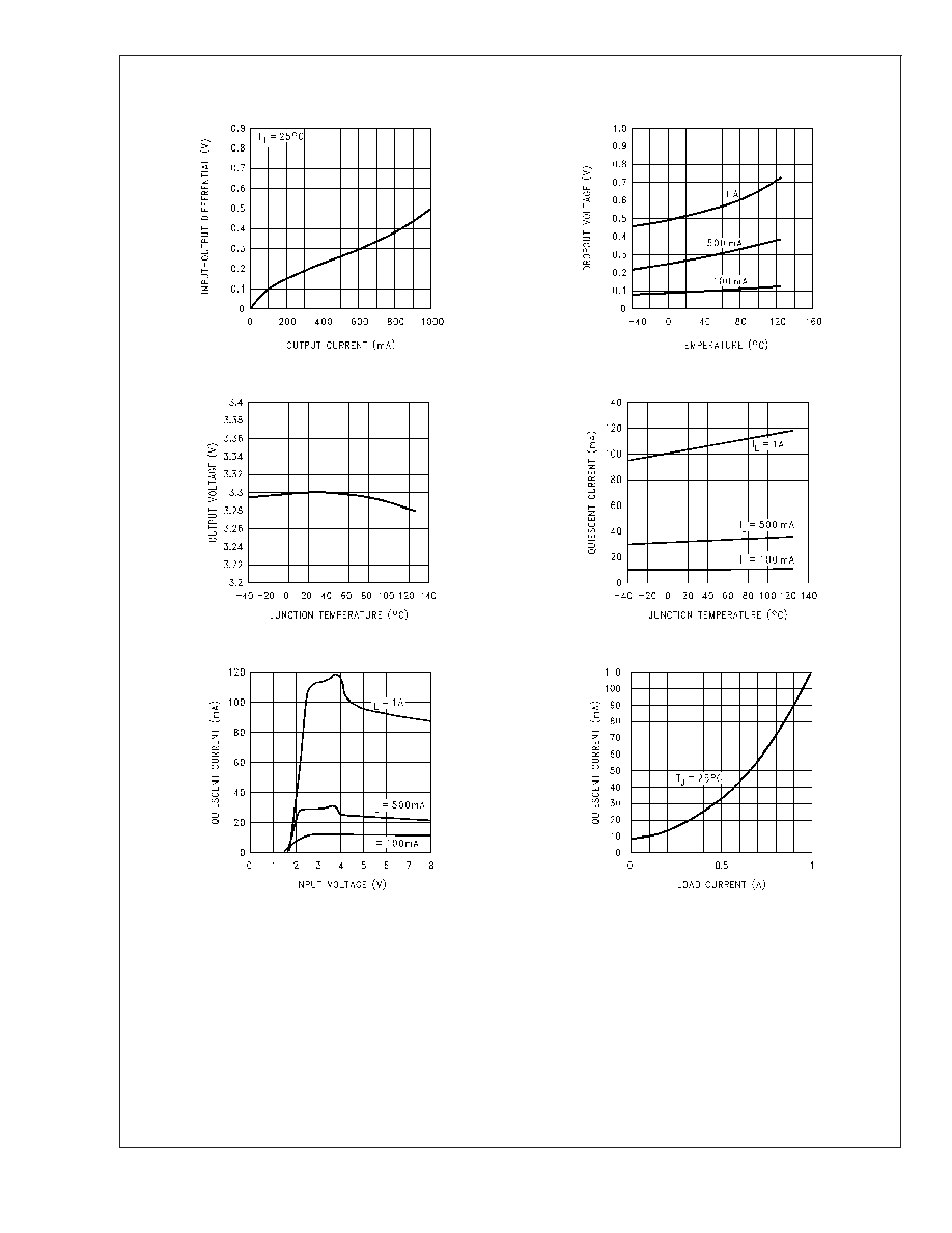
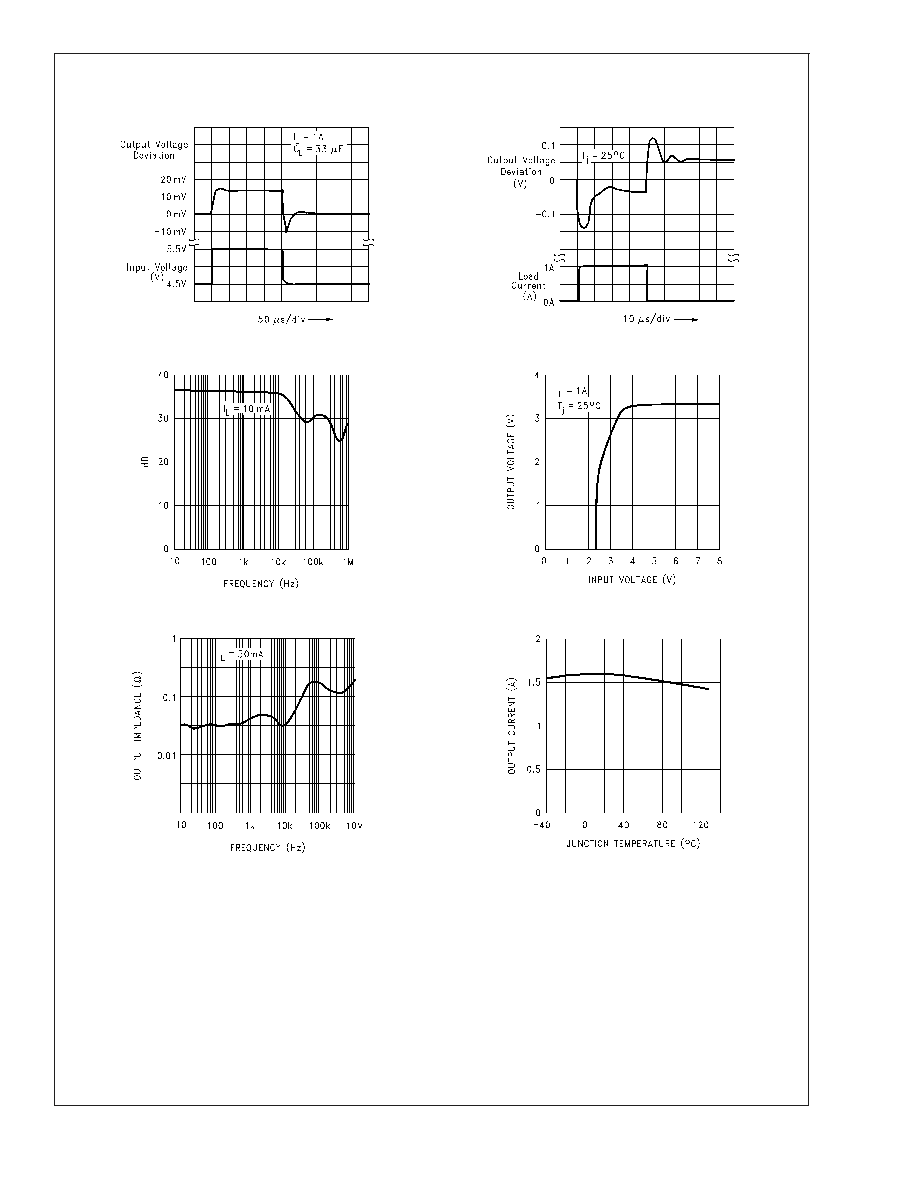
Typical Performance Characteristics
Dropout Voltage
Dropout Voltage vs. Temperature
01208013
01208014
Output Voltage vs. Temperature
Quiescent Current vs. Temperature
01208015
01208016
Quiescent Current vs. V
IN
Quiescent Current vs. Load
01208017
01208018
LM3940
www.national.com
4