LM4051
Precision Micropower Shunt Voltage Reference
General Description
Ideal for space critical applications, the LM4051 precision
voltage reference is available in the sub-miniature (3 mm x
1.3 mm) SSOT-23 surface-mount package. The LM4051's
advanced design eliminates the need for an external stabiliz-
ing capacitor while ensuring stability with any capacitive
load, thus making the LM4051 easy to use. Further reducing
design effort is the availability of a fixed (1.225V) and adjust-
able reverse breakdown voltage. The minimum operating
current is 60 µA for the LM4051-1.2 and the LM4051-ADJ.
Both versions have a maximum operating current of 12 mA.
The LM4051 comes in three grades (A, B, and C). The best
grade devices (A) have an initial accuracy of 0.1%, while the
B-grade have 0.2% and the C-grade 0.5%, all with a tempco
of 50 ppm/∞C guaranteed from -40∞C to 125∞C.
The LM4051 utilizes fuse and zener-zap trim of reference
voltage during wafer sort to ensure that the prime parts have
an accuracy of better than
±
0.1% (A grade) at 25∞C.
Features
n
Small packages: SSOT-23
n
No output capacitor required
n
Tolerates capacitive loads
n
Reverse breakdown voltage options of 1.225V and
adjustable
Key Specifications (LM4051-1.2)
n
Output voltage tolerance
(A grade, 25∞C)
±
0.1%(max)
n
Low output noise
(10 Hz to 10kHz)
20µV
rms
n
Wide operating current range
60µA to 12mA
n
Industrial temperature range
(tempco guaranteed from
-40∞C to +125∞C)
-40∞C to +85∞C
n
Low temperature coefficient
50 ppm/∞C (max)
Applications
n
Portable, Battery-Powered Equipment
n
Data Acquisition Systems
n
Instrumentation
n
Process Control
n
Energy Management
n
Automotive and Industrial
n
Precision Audio Components
n
Base Stations
n
Battery Chargers
n
Medical Equipment
n
Communication
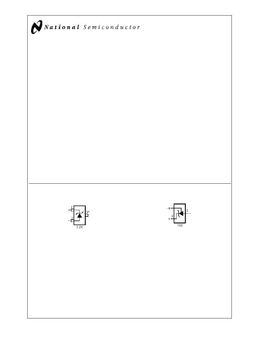
Connection Diagrams
SSOT-23
DS101222-1
*This pin must be left floating or connected to pin 2.
DS101222-40
Top View
See NS Package Number MF03A
February 2000
LM4051
Precision
Micropower
Shunt
V
oltage
Reference
© 2000 National Semiconductor Corporation
DS101222
www.national.com
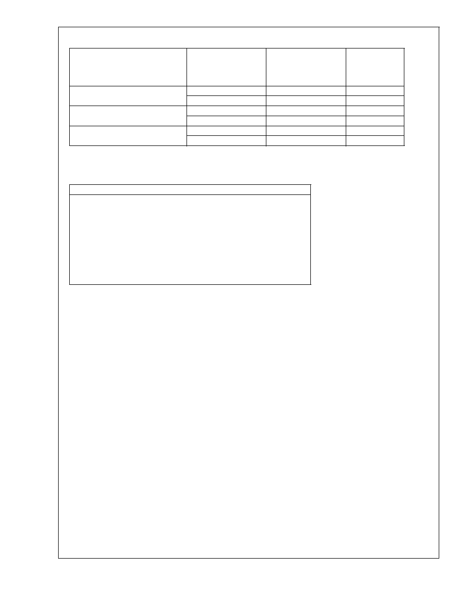
Ordering Information
Reverse Breakdown
Voltage Tolerance at 25∞C and
Average Reverse Breakdown
Voltage Temperature Coefficient
LM4051 Supplied as
1000 Units, Tape and
Reel
LM4051 Supplied as
3000 Units, Tape and
Reel
Part Marking
±
0.1%, 50 ppm/∞C max (A grade)
LM4051AIM3-1.2
LM4051AIM3X-1.2
RIA
LM4051AIM3-ADJ
LM4051AIM3X-ADJ
RHA
±
0.2%, 50 ppm/∞C max (B grade)
LM4051BIM3-1.2
LM4051BIM3X-1.2
RIB
LM4051BIM3-ADJ
LM4051BIM3X-ADJ
RHB
±
0.5%, 50 ppm/∞C max (C grade)
LM4051CIM3-1.2
LM4051CIM3X-1.2
RIC
LM4051CIM3-ADJ
LM4051CIM3X-ADJ
RHC
SOT-23 Package Marking Information
Only three fields of marking are possible on the SSOT-23's small surface. This
table gives the meaning of the three fields.
Field Definition
First Field:
R = Reference
Second Field:
I = 1.225V Voltage Option
H = Adjustable
Third Field:
A≠C = Initial Reverse Breakdown
Voltage or Reference Voltage Tolerance
A =
±
0.1%, B =
±
0.2%, C =
±
0.5%
LM4051
www.national.com
2
Absolute Maximum Ratings
(Note 1)
If Military/Aerospace specified devices are required,
please contact the National Semiconductor Sales Office/
Distributors for availability and specifications.
Reverse Current
20 mA
Forward Current
10 mA
Maximum Output Voltage
(LM4051-ADJ)
15V
Power Dissipation (T
A
= 25∞C) (Note 2)
M3 Package
280 mW
Storage Temperature
-65∞C to +150∞C
Lead Temperature
M3 Packages
Vapor phase (60 seconds)
+215∞C
Infrared (15 seconds)
+220∞C
ESD Susceptibility
Human Body Model (Note 3)
2 kV
Machine Model (Note 3)
200V
See AN-450 "Surface Mounting Methods and Their Effect
on Product Reliability" for other methods of soldering
surface mount devices.
Operating Ratings
(Notes 1, 2)
Temperature Range
(T
min
T
A
T
max
)
Industrial Temperature Range
-40∞C
T
A
+85∞C
Reverse Current
LM4051-1.2
60 µA to 12 mA
LM4051-ADJ
60 µA to 12 mA
Output Voltage Range
LM4051-ADJ
1.24V to 10V
LM4051-1.2
Electrical Characteristics
Boldface limits apply for T
A
= T
J
= T
MIN
to T
MAX
; all other limits T
A
= T
J
= 25∞C. The grades A, B and C designate initial Re-
verse Breakdown Voltage tolerances of
±
0.1%,
±
0.2% and
±
0.5% respectively.
Symbol
Parameter
Conditions
Typical
(Note 4)
LM4051AIM3
(Limits)
(Note 5)
LM4051BIM3
(Limits)
(Note 5)
LM4051CIM3
Limts
(Note 5)
Units
(Limit)
V
R
Reverse Breakdown
Voltage
I
R
= 100 µA
1.225
V
Reverse Breakdown
Voltage
I
R
= 100 µA
±
1.2
±
2.4
±
6
mV (max)
Tolerance (Note 6)
±
5.2
±
6.4
±
10.1
mV (max)
I
RMIN
Minimum Operating
Current
39
µA
60
60
60
µA (max)
65
65
65
µA (max)
V
R
/
T
Average Reverse
Breakdown
Voltage Temperature
Coefficient (Note 6)
I
R
= 10 mA
±
20
ppm/∞C
I
R
= 1 mA
±
15
ppm/∞C
I
R
= 100 µA
T = -40∞C to 125∞C
±
15
±
50
±
50
±
50
ppm/∞C
(max)
V
R
/
I
R
Reverse Breakdown
Voltage
Change with Operating
Current Change
I
RMIN
I
R
1 mA
0.3
mV
1.1
1.1
1.1
mV (max)
1.5
1.5
1.5
mV (max)
1 mA
I
R
12 mA
1.8
mV
6.0
6.0
6.0
mV (max)
8.0
8.0
8.0
mV (max)
Z
R
Reverse Dynamic
Impedance
I
R
= 1 mA, f = 120 Hz
0.5
e
N
Wideband Noise
I
R
= 100 µA
20
µV
rms
10 Hz
f
10 kHz
V
R
Reverse Breakdown
Voltage
Long Term Stability
(Note 9)
t = 1000 hrs
T = 25∞C
±
0.1∞C
I
R
= 100 µA
120
ppm
V
HYST
Output Hysteresis
(Note 10)
T = -40∞C to 125∞C
0.36
mV/V
LM4051
www.national.com
3
LM4051-ADJ (Adjustable)
Electrical Characteristics
Boldface limits apply for T
A
= T
J
= T
MIN
to T
MAX
; all other limits T
J
= 25∞C unless otherwise specified (SSOT-23, see (Note 7)
, I
RMIN
I
R
12 mA, V
REF
V
OUT
10V. The grades A, B and C designate initial Reference Voltage Tolerances of
±
0.1%,
±
0.2% and
±
0.5%, respectively for V
OUT
= 5V.
Symbol
Parameter
Conditions
Typical
(Note 4)
LM4051AIM3
(Note 5)
LM4051BIM3
(Note 5)
LM4051CIM3
(Note 5)
Units
(Limit)
V
REF
Reference Voltage
I
R
= 100 µA, V
OUT
= 5V
1.212
V
Reference Voltage
Tolerance (Note 6),
(Note 8)
I
R
= 100 µA, V
OUT
= 5V
±
1.2
±
5.2
±
2.4
±
6.4
±
6
±
10.1
mV (max)
mV (max)
I
RMIN
Minimum Operating
Current
36
60
65
60
65
65
70
µA
µA (max)
µA (max)
V
REF
/
I
R
Reference
VoltageChange with
Operating Current
Change
I
RMIN
I
R
1mA
V
OUT
1.6V
(Note 7)
0.3
1.1
1.5
1.1
1.5
1.1
1.5
mV
mV (max)
mV(max)
1 mA
I
R
12 mA
V
OUT
1.6V(Note 7)
0.6
6
8
6
8
6
8
mV
mV (max)
mV (max)
V
REF
/
V
O
Reference Voltage
Changewith Output
Voltage Change
I
R
= 0.1 mA
-1.69
-2.8
-3.5
-2.8
-3.5
-2.8
-3.5
mV/V
mV/V (max)
mV/V (max)
I
FB
Feedback Current
70
130
150
130
150
130
150
nA
nA (max)
nA (max)
V
REF
/
T
Average
ReferenceVoltage
Temperature
Coefficient (Note 8)
V
OUT
= 2.5V
I
R
= 10mA
20
ppm/∞C
I
R
= 1mA
15
ppm/∞C
I
R
= 100µA
15
±
50
±
50
±
50
ppm/∞C
(max)
T = -40∞C to +125∞C
Z
OUT
Dynamic Output
Impedance
I
R
= 1 mA,
f = 120 Hz,
I
AC
= 0.1 I
R
V
OUT
= V
REF
V
OUT
= 10V
0.3
2
e
N
Wideband Noise
I
R
= 100 µA
V
OUT
= V
REF
10 Hz
f
10 kHz
20
µV
rms
V
REF
Reference Voltage
Long Term Stability
(Note 9)
t = 1000 hrs,
I
R
= 100 µA
T = 25∞C
±
0.1∞C
120
ppm
V
HYST
Output Hysteresis
(Note 10)
T = -40∞C to +125∞C
0.3
mV/V
LM4051
www.national.com
4
Electrical Characteristics (continued)
Note 1: Absolute Maximum Ratings indicate limits beyond which damage to the device may occur. Operating Ratings indicate conditions for which the device is
functional, but do not guarantee specific performance limits. For guaranteed specifications and test conditions, see the Electrical Characteristics. The guaranteed
specifications apply only for the test conditions listed. Some performance characteristics may degrade when the device is not operated under the listed test condi-
tions.
Note 2: The maximum power dissipation must be derated at elevated temperatures and is dictated by T
Jmax
(maximum junction temperature),
JA
(junction to am-
bient thermal resistance), and T
A
(ambient temperature). The maximum allowable power dissipation at any temperature is PD
max
= (T
Jmax
- T
A
)/
JA
or the number
given in the Absolute Maximum Ratings, whichever is lower. For the LM4051, T
Jmax
= 125∞C, and the typical thermal resistance (
JA
), when board mounted, is
280∞C/W for the SSOT-23 package.
Note 3: The human body model is a 100 pF capacitor discharged through a 1.5 k
resistor into each pin. The machine model is a 200 pF capacitor discharged di-
rectly into each pin.
Note 4: Typicals are at T
J
= 25∞C and represent most likely parametric norm.
Note 5: Limits are 100% production tested at 25∞C. Limits over temperature are guaranteed through correlation using Statistical Quality Control (SQC) methods.
The limits are used to calculate National's AOQL.
Note 6: The boldface (over-temperature) limit for Reverse Breakdown Voltage Tolerance is defined as the room temperature Reverse Breakdown Voltage Tolerance
±
[(
V
R
/
T)(max
T)(V
R
)]. Where,
V
R
/
T is the V
R
temperature coefficient, max
T is the maximum difference in temperature from the reference point of 25 ∞C to
T
MAX
or T
MIN
, and V
R
is the reverse breakdown voltage. The total over-temperature tolerance for the different grades in the industrial temperature range where
max
T=65∞C is shown below:
A-grade:
±
0.425% =
±
0.1%
±
50 ppm/∞C x 65∞C
B-grade:
±
0.522% =
±
0.2%
±
50 ppm/∞C x 65∞C
C-grade:
±
0.825% =
±
0.5%
±
50 ppm/∞C x 65∞C
Therefore, as an example, the A-grade LM4051-1.2 has an over-temperature Reverse Breakdown Voltage tolerance of
±
1.2V x 0.425% =
±
5.2 mV.
Note 7: When V
OUT
1.6V, the LM4051-ADJ in the SSOT-23 package must operate at reduced I
R
. This is caused by the series resistance of the die attach between
the die (-) output and the package (-) output pin. See the Output Saturation curve in the Typical Performance Characteristics section.
Note 8: Reference voltage and temperature coefficient will change with output voltage. See Typical Performance Characteristics curves.
Note 9: Long term stability is V
R
@
25∞C measured during 1000 hrs.
Note 10: Thermal hysteresis is defined as the changes in 25∞C output voltage before and after cycling the device from -40∞C or +125∞C.
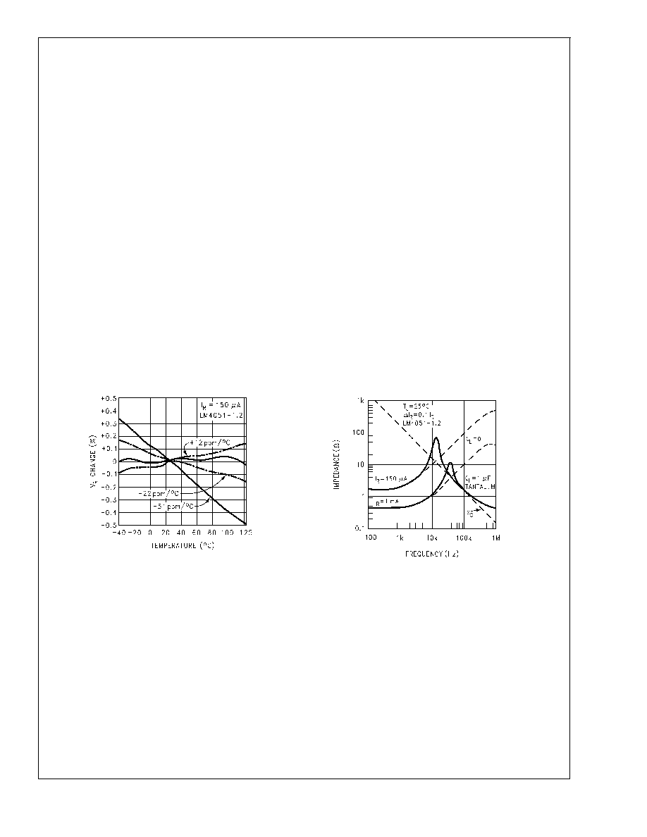
Typical Performance Characteristics
Temperature Drift for Different
Average Temperature Coefficient
DS101222-19
Output Impedance vs Frequency
DS101222-4
LM4051
www.national.com
5