 | ÐлекÑÑоннÑй компоненÑ: LM40CIMT | СкаÑаÑÑ:  PDF PDF  ZIP ZIP |
Äîêóìåíòàöèÿ è îïèñàíèÿ www.docs.chipfind.ru
LM40
Hardware Monitor with Dual Thermal Diodes and
SensorPath
TM
Bus
General Description
The LM40 is a hardware monitor that measures 3 tempera-
ture zones, 5 voltages and has a single-wire interface com-
patible with National Semiconductor's SensorPath bus. Sen-
sorPath data is pulse width encoded, thereby allowing the
LM40 to be easily connected to many general purpose
micro-controllers. Several National Semiconductor Super I/O
products include a fully integrated SensorPath master, that
when connected to the LM40 can realize a hardware monitor
function that includes limit checking for measured values,
autonomous fan speed control and many other functions.
The LM40 measures the temperature of its own die as well
as two external devices such as a processor thermal diode
or a diode connected transistor. The LM40 can resolve tem-
peratures up to 255°C and down to -256°C. The operating
temperature range of the LM40 is 0°C to +125°C. Using
ADC it measures +1.2V, +2.5V, +3.3V, +5V and +12V analog
input voltages with internal scaling resistors.The address
programming pin allows two LM40s to be placed on one
SensorPath bus.
Features
n
SensorPath Interface
-- 2 hardware programmable addresses
n
Voltage Monitoring
-- 9-bit
ADC
-- Internal scaling resistors for all inputs
-- Monitors +1.2V, +2.5 V, +3.3 V, +5 V and +12 V
n
Temperature Sensing
-- 2 remote diode temperature sensor zones
-- Internal local temperature zone
-- 0.5 °C resolution
-- Measures temperatures up to 140 °C
n
14-lead TSSOP package
Key Specifications
n
Voltage Measurement Accuracy
±
2 % (max)
n
Temperature Sensor Accuracy
±
3 °C (max)
n
Temperature Range:
-- LM40 junction
0 °C to +85 °C
-- Remote Temp Accuracy
0 °C to +100 °C
n
Power Supply Voltage
+3.0 V to +3.6 V
n
Average Power Supply Current
0.5 mA (typ)
n
Conversion Time (all Channels)
29.6ms to 1456ms
Applications
n
Microprocessor based equipment
(Motherboards, Video Cards, Base-stations, Routers,
ATMs, Point of Sale, ...)
n
Power Supplies
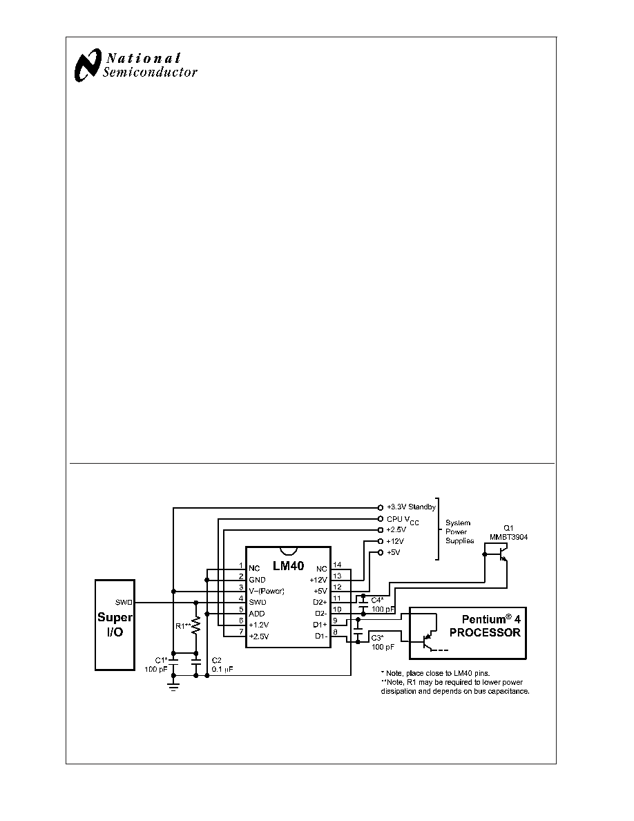
Typical Application
20068401
SensorPath
TM
is a trademark of National Semiconductor Corporation
May 2004
LM40
Hardware
Monitor
with
Dual
Thermal
Diodes
and
SensorPath
TM
Bus
© 2004 National Semiconductor Corporation
DS200684
www.national.com
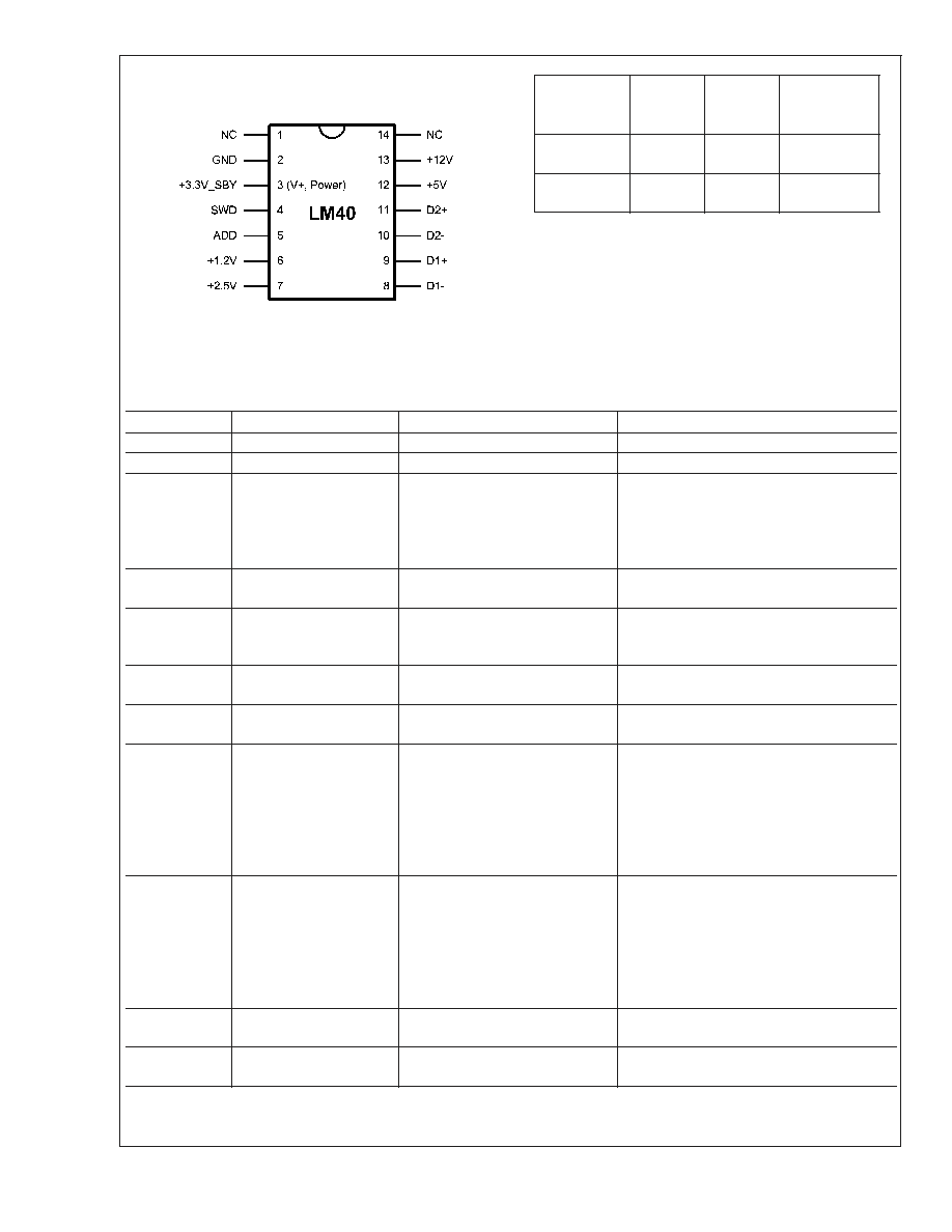
Connection Diagram
TSSOP-14
20068402
Top View
National Package Number MTC14C
Order
Number
Package
Marking
NS
Package
Number
Transport
Media
LM40CIMT
LM40
CIMT
MTC14C
94 units per
rail
LM40CIMTX
LM40
CIMT
MTC14C
2500 units in
tape and reel
Pin Description
Pin Number
Pin Name
Description
Typical Connection
1, 14
NC
No Connect
May be tied to V+, GND or left floating
2
GND
Ground
System ground
3
V+/+3.3V_SBY
Positive power supply pin as well
as a +3.3V voltage monitor
Connected system 3.3 V standby power and
to a 0.1 µF bypass capacitor in parallel with
100 pF. A bulk capacitance of approximately
10 µF needs to be in the near vicinity of the
LM40.
4
SWD
SensorPath Bus line; Open-drain
output
Super I/O, Pull-up resistor, 1.6k
5
ADD
Digital input - device number select
input for the serial bus device
number
Pull-up to 3.3 V or pull-down to GND resistor,
10k; must never be left floating
6
+1.2V
+1.2V voltage monitoring input with
scaling resistors
Processor core voltage to be monitored
7
+2.5V
+2.5V voltage monitoring input with
scaling resistors
Power supply voltage to be monitored
8, 10
D1-, D2-
Thermal diode analog voltage
output and negative monitoring
input
Remote Thermal Diode cathode
(THERM_DC) - Diode 1 should always be
connected to the processor thermal diode.
Diode 2 may be connected to an MMBT3904
or GPU thermal diode. A 100 pF capacitor
should be connected between respective D-
and D+ for noise filtering.
9, 11
D1+, D2+
Thermal diode analog current
output and positive monitoring input
Remote Thermal Diode anode (THERM_DA) -
Diode 1 should always be connected to the
processor thermal diode. Diode 2 may be
connected to an MMBT3904 or GPU thermal
diode. A 100 pF capacitor should be
connected between respective D- and D+ for
noise filtering.
12
+5V
+5V voltage monitoring input with
scaling resistors
Power supply voltage to be monitored
13
+12V
+12V voltage monitoring input with
scaling resistors
Power supply voltage to be monitored
LM40
www.national.com
2
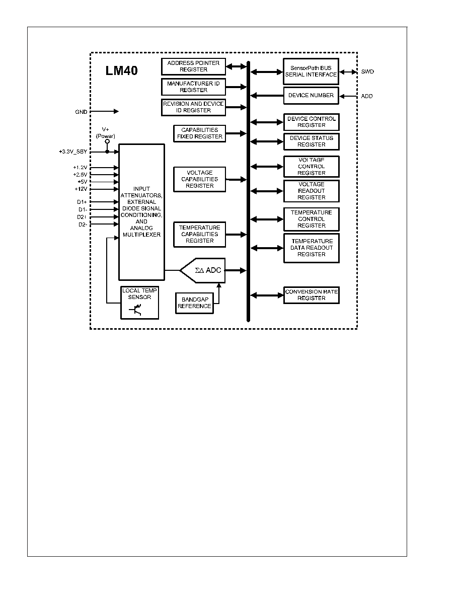
Block Diagram
20068403
LM40
www.national.com
3

Absolute Maximum Ratings
(Notes 2, 1)
Supply Voltage (V
+
)
-0.5 V to 6.0 V
Voltage at Any Digital Input or
Output Pin
-0.5 V to 6.0 V
Voltage on 12V Analog Input
-0.5 V to 16 V
Voltage on 5V Analog Input
-0.5 V to 6.67 V
Voltage on D1+ and D2+
-0.5 V to (V+ + 0.05 V)
Voltage on Other Analog Inputs
-0.5 V to 6.0 V
Current on D1- and D2-
±
1 mA
Input Current per Pin(Note 3)
±
5 mA
Package Input Current (Note 3)
±
30 mA
Package Power Dissipation
(Note 4)
Output Sink Current
10 mA
ESD Susceptibility (Note 5)
Human Body Model
2500 V
Machine Model
250 V
Storage Temperature
-65°C to +150°C
Soldering process must comply with National's reflow
temperature profile specifications. Refer to
www.national.com/packaging/. (Note 6)
Operating Ratings
(Notes 1, 2)
Temperature Range for Electrical Characteristics
LM40CIMT (T
MIN
T
A
T
MAX
)
0°C
T
A
+85°C
Operating Temperature Range
0°C
T
A
+125°C
Remote Diode Temperature (T
D
)
Range
-5 °C
T
D
+140 °C
Supply Voltage Range (V+)
+3.0 V to +3.6 V
Analog Input Voltage Rage:
+1.2V and +2.5V
-0.05V to
(V+ + 0.05V)
+3.3V_SBY (V+)
+3.0V to +3.6V
+5V
-0.05V to +6.67V
+12V
-0.05V to +16V
DC Electrical Characteristics
The following specifications apply for V+ = +3.0 V
DC
to +3.6 V
DC
, and all analog source impedance R
S
= 50
unless other-
wise specified in the conditions. Boldface limits apply for LM40CIMT T
A
= T
J
= T
MIN
=0°C to T
MAX
=85°C; all other limits
T
A
= +25°C. T
A
is the ambient temperature of the LM40; T
J
is the junction temperature of the LM40; T
D
is the junction tem-
perature of the remote thermal diode.
POWER SUPPLY CHARACTERISTICS
Symbol
Parameter
Conditions
Typical
(Note 7)
Limits
(Note 8)
Units
(Limit)
V+
Power Supply Voltage
3.3
3.0
3.6
V (min)
V (max)
I+
Shutdown
Shutdown Power Supply Current
SensorPath Bus Inactive
(Note 9)
260
420
µA (max)
I+
Average
Average Power Supply Current
SensorPath Bus Inactive; all
sensors enabled;
t
CONV
=182 ms; (Note 9)
900
µA (max)
I+
Peak
Peak Power Supply Current
SensorPath Bus Inactive
(Note 9)
3.3
mA (max)
Power-On Reset Threshold Voltage
1.6
V (min)
2.8
V (max)
TEMPERATURE-TO-DIGITAL CONVERTER CHARACTERISTICS
Parameter
Conditions
Typical
(Note 7)
Limits
(Note 8)
Units
(Limits)
Temperature Accuracy Using the Remote Thermal
Diode, see (Note 12) for Thermal Diode Processor
Type.
T
J
= 0°C to
+85°C
T
D
= +25°C
±
1
±
2.5
°C (max)
T
J
= 0°C to
+85°C
T
D
= 0°C to
+100°C
±
3
°C (max)
TJ = 0°C to
+85°C
T
D
= +100°C to
+125°C
±
4
°C (max)
Temperature Accuracy Using the Local Diode
T
J
= 0°C to +85°C (Note 10)
±
1
±
3
°C (max)
Remote Diode and Local Temperature Resolution
10
Bits
0.5
°C
D- Source Voltage
0.7
V
LM40
www.national.com
4

TEMPERATURE-TO-DIGITAL CONVERTER CHARACTERISTICS
Parameter
Conditions
Typical
(Note 7)
Limits
(Note 8)
Units
(Limits)
Diode Source Current
(V
D+
- V
D-
) = +0.65 V; High Current
188
280
µA (max)
Low Current
11.75
µA
Diode Source Current High Current to Low Current
Ratio
16
ANALOG TO DIGITAL CONVERTER CHARACTERISTICS
Symbol
Parameter
Conditions
Typical
(Note 7)
Limits
(Note 8)
Units
(Limit)
TUE
Total Unadjusted Error(Note 11)
±
2
%FS
(max)
Resolution
9
Bits
DNL
Differential Non-linearity
1
LSB
Power Supply Sensitivity
±
1
%/V
Input Resistance, all analog inputs (total resistance
of divider chain)
210
140
k
(min)
400
k
(max)
SWD and ADD DIGITAL INPUT CHARACTERISTICS
Symbol
Parameter
Conditions
Typical
(Note 7)
Limits
(Note 8)
Units
(Limit)
V
IH
SWD Logical High Input Voltage
2.1
V (min)
V+ + 0.5
V (max)
V
IL
SWD Logical Low Input Voltage
0.8
V (max)
-0.5
V (min)
V
IH
ADD Logical High Input Voltage
90% x V+
V (min)
V
IL
ADD Logical Low Input Voltage
10% x V+
V (max)
V
HYST
Input Hysteresis
300
mV
I
L
SWD and ADD Input Current
GND
V
IN
V+
±
0.005
±
10
µA (max)
SWD Input Current with V+ Open or
Grounded
GND
V
IN
3.6V,
and V+ Open or
GND
±
0.005
µA
C
IN
Digital Input Capacitance
10
pF
SWD DIGITAL OUTPUT CHARACTERISTICS
Symbol
Parameter
Conditions
Typical
(Note 7)
Limits
(Note 8)
Units
(Limit)
V
OL
Open-drain Output Logic "Low"
Voltage
I
OL
= 4mA
0.4
V (max)
I
OL
= 50µA
0.2
V (max)
I
OH
Open-drain Output Off Current
±
0.005
±
10
µA (max)
C
OUT
Digital Output Capacitance
10
pF
AC Electrical Characteristics
The following specification apply for V+ = +3.0 V
DC
to +3.6 V
DC
, unless otherwise specified. Boldface limits apply for
T
A
= T
J
= T
MIN
=0°C to T
MAX
=85°C; all other limits T
A
= T
J
= 25°C. The SensorPath Characteristics conform to the SensorPath
specification revision 0.98. Please refer to that speciation for further details.
Symbol
Parameter
Conditions
Typical
(Note 7)
Limits
(Note 8)
Units
(Limits)
HARDWARE MONITOR CHARACTERISTICS
t
CONV
Total Monitoring Cycle Time (Note 13)
All Voltage and
Temperature readings
(Default)
182
163.8
ms (min)
200.2
ms (max)
SensorPath Bus CHARACTERISTICS
t
f
SWD fall time (Note 16)
R
pull-up
=1.25 k
±
30%,
C
L
=400 pF
300
ns (max)
LM40
www.national.com
5
Document Outline