 | –≠–ª–µ–∫—Ç—Ä–æ–Ω–Ω—ã–π –∫–æ–º–ø–æ–Ω–µ–Ω—Ç: LM4250CJ | –°–∫–∞—á–∞—Ç—å:  PDF PDF  ZIP ZIP |

LM4250
Programmable Operational Amplifier
General Description
The LM4250 and LM4250C are extremely versatile program-
mable monolithic operational amplifiers. A single external
master bias current setting resistor programs the input bias
current, input offset current, quiescent power consumption,
slew rate, input noise, and the gain-bandwidth product. The
device is a truly general purpose operational amplifier.
The LM4250C is identical to the LM4250 except that the
LM4250C has its performance guaranteed over a 0∞C to
+70∞C temperature range instead of the -55∞C to +125∞C
temperature range of the LM4250.
Features
n
±
1V to
±
18V power supply operation
n
3 nA input offset current
n
Standby power consumption as low as 500 nW
n
No frequency compensation required
n
Programmable electrical characteristics
n
Offset voltage nulling capability
n
Can be powered by two flashlight batteries
n
Short circuit protection
Connection Diagrams
Metal Can Package
DS009300-2
Top View
Dual-In-Line Package
DS009300-5
Top View
X5 Difference Amplifier
DS009300-3
Quiescent P
D
= 0.6 mW
500 Nano-Watt X10 Amplifier
DS009300-4
Quiescent P
D
= 500 nW
August 2000
LM4250
Programmable
Operational
Amplifier
© 2000 National Semiconductor Corporation
DS009300
www.national.com

Absolute Maximum Ratings
(Note 1)
If Military/Aerospace specified devices are required,
please contact the National Semiconductor Sales Office/
Distributors for availability and specifications.
(Note 3)
LM4250
LM4250C
Supply Voltage
±
18V
±
18V
Operating Temp. Range
-55∞C
T
A
+125∞C
0∞C
T
A
+70∞C
Differential Input Voltage
±
30V
±
30V
Input Voltage (Note 2)
±
15V
±
15V
I
SET
Current
150 nA
150 nA
Output Short Circuit Duration
Continuous
Continuous
T
JMAX
H-Package
150∞C
100∞C
N-Package
100∞C
J-Package
150∞C
100∞C
M-Package
100∞C
Power Dissipation at T
A
= 25∞C
H-Package (Still Air)
500 mW
300 mW
(400 LF/Min Air Flow)
1200 mW
1200 mW
N-Package
500 mW
J-Package
1000 mW
600 mW
M-Package
350 mW
Thermal Resistance (Typical)
JA
H-Package (Still Air)
165∞C/W
165∞C/W
(400 LF/Min Air Flow)
65∞C/W
65∞C/W
N-Package
130∞C/W
J-Package
108∞C/W
108∞C/W
M-Package
190∞C/W
(Typical)
JC
H-Package
21∞C/W
21∞C/W
Storage Temperature Range
-65∞C to +150∞C
-65∞C to +150∞C
Soldering Information
Dual-In-Line Package
Soldering (10 seconds)
260∞C
Small Outline Package
Vapor Phase (60 seconds)
215∞C
Infrared (15 seconds)
220∞C
See AN-450 "Surface Mounting Methods and Their Effect
on Product Reliability" for other methods of soldering
surface mount devices.
ESD tolerance (Note 4)
800V
Note 1: "Absolute Maximum Ratings" indicate limits beyond which damage
to the device may occur. Operating Ratings indicate conditions for which the
device is functional, but do not guarantee specific performance limits.
Note 2: For supply voltages less than
±
15V, the absolute maximum input
voltage is equal to the supply voltage.
Note 3: Refer to RETS4250X for military specifications.
Note 4: Human body model, 1.5 k
in series with 100 pF.
LM4250
www.national.com
2
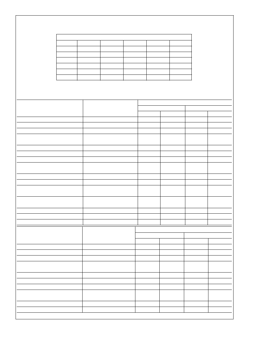
Resistor Biasing
Set Current Setting Resistor to V
-
I
SET
V
S
0.1 µA
0.5 µA
1.0 µA
5 µA
10 µA
±
1.5V
25.6 M
5.04 M
2.5 M
492 k
244 k
±
3.0V
55.6 M
11.0 M
5.5 M
1.09 M
544 k
±
6.0V
116 M
23.0 M
11.5 M
2.29 M
1.14 M
±
9.0V
176 M
35.0 M
17.5 M
3.49 M
1.74 M
±
12.0V
236 M
47.0 M
23.5 M
4.69 M
2.34 M
±
15.0V
296 M
59.0 M
29.5 M
5.89 M
2.94 M
Electrical Characteristics
LM4250 (-55∞C
T
A
+125∞C unless otherwise specified.) T
A
= T
J
V
S
=
±
1.5V
Parameter
Conditions
I
SET
= 1 µA
I
SET
= 10 µA
Min
Max
Min
Max
V
OS
R
S
100 k
, T
A
= 25∞C
3 mV
5 mV
I
OS
T
A
= 25∞C
3 nA
10 nA
I
bias
T
A
= 25∞C
7.5 nA
50 nA
Large Signal Voltage
R
L
= 100 k
, T
A
= 25∞C
40k
Gain
V
O
=
±
0.6V, R
L
= 10 k
50k
Supply Current
T
A
= 25∞C
7.5 µA
80 µA
Power Consumption
T
A
= 25∞C
23 µW
240 µW
V
OS
R
S
100 k
4 mV
6 mV
I
OS
T
A
= +125∞C
5 nA
10 nA
T
A
= -55∞C
3 nA
10 nA
I
bias
7.5 nA
50 nA
Input Voltage Range
±
0.6V
±
0.6V
Large Signal Voltage Gain
V
O
=
±
0.5V, R
L
= 100 k
30k
R
L
= 10 k
30k
Output Voltage Swing
R
L
= 100 k
±
0.6V
R
L
= 10 k
±
0.6V
Common Mode Rejection Ratio
R
S
10 k
70 dB
70 dB
Supply Voltage Rejection Ratio
R
S
10 k
76 dB
76 dB
Supply Current
8 µA
90 µA
V
S
=
±
15V
Parameter
Conditions
I
SET
= 1 µA
I
SET
= 10 µA
Min
Max
Min
Max
V
OS
R
S
100 k
, T
A
= 25∞C
3 mV
5 mV
I
OS
T
A
= 25∞C
3 nA
10 nA
I
bias
T
A
= 25∞C
7.5 nA
50 nA
Large Signal Voltage
R
L
= 100 k
, T
A
= 25∞C
100k
Gain
V
O
=
±
10V, R
L
= 10 k
100k
Supply Current
T
A
= 25∞C
10 µA
90 µA
Power Consumption
T
A
= 25∞C
300 µW
2.7 mW
V
OS
R
S
100 k
4 mV
6 mV
I
OS
T
A
= +125∞C
25 nA
25 nA
T
A
= -55∞C
3 nA
10 nA
I
bias
7.5 nA
50 nA
Input Voltage Range
±
13.5V
±
13.5V
LM4250
www.national.com
3
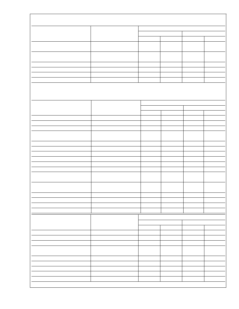
Electrical Characteristics
(Continued)
V
S
=
±
15V
Parameter
Conditions
I
SET
= 1 µA
I
SET
= 10 µA
Min
Max
Min
Max
Large Signal Voltage
V
O
=
±
10V, R
L
= 100 k
50k
Gain
R
L
= 10 k
50k
Output Voltage Swing
R
L
= 100 k
±
12V
R
L
= 10 k
±
12V
Common Mode Rejection Ratio
R
S
10 k
70 dB
70 dB
Supply Voltage Rejection Ratio
R
S
10 k
76 dB
76 dB
Supply Current
11 µA
100 µA
Power Consumption
330 µW
3 mW
Electrical Characteristics
LM4250C (0∞C
T
A
+70∞C unless otherwise specified.) T
A
= T
J
V
S
=
±
1.5V
Parameter
Conditions
I
SET
= 1 µA
I
SET
= 10 µA
Min
Max
Min
Max
V
OS
R
S
100 k
, T
A
= 25∞C
5 mV
6 mV
I
OS
T
A
= 25∞C
6 nA
20 nA
I
bias
T
A
= 25∞C
10 nA
75 nA
Large Signal Voltage Gain
R
L
= 100 k
, T
A
= 25∞C
25k
V
O
=
±
0.6V, R
L
= 10 k
25k
Supply Current
T
A
= 25∞C
8 µA
90 µA
Power Consumption
T
A
= 25∞C
24 µW
270 µW
V
OS
R
S
10 k
6.5 mV
7.5 mV
I
OS
8 nA
25 nA
I
bias
10 nA
80 nA
Input Voltage Range
±
0.6V
±
0.6V
Large Signal Voltage
V
O
=
±
0.5V, R
L
= 100 k
25k
Gain
R
L
= 10 k
25k
Output Voltage Swing
R
L
= 100 k
±
0.6V
R
L
= 10 k
±
0.6V
Common Mode Rejection Ratio
R
S
10 k
70 dB
70 dB
Supply Voltage Rejection Ratio
R
S
10 k
74 dB
74 dB
Supply Current
8 µA
90 µA
Power Consumption
24 µW
270 µW
V
S
=
±
15V
Parameter
Conditions
I
SET
= 1 µA
I
SET
= 10 µA
Min
Max
Min
Max
V
OS
R
S
100 k
, T
A
= 25∞C
5 mV
6 mV
I
OS
T
A
= 25∞C
6 nA
20 nA
I
bias
T
A
= 25∞C
10 nA
75 nA
Large Signal Voltage
R
L
= 100 k
, T
A
= 25∞C
60k
Gain
V
O
=
±
10V, R
L
= 10 k
60k
Supply Current
T
A
= 25∞C
11 µA
100 µA
Power Consumption
T
A
= 25∞C
330 µW
3 mW
V
OS
R
S
100 k
6.5 mV
7.5 mV
I
OS
8 nA
25 nA
I
bias
10 nA
80 nA
LM4250
www.national.com
4
Electrical Characteristics
(Continued)
V
S
=
±
15V
Parameter
Conditions
I
SET
= 1 µA
I
SET
= 10 µA
Min
Max
Min
Max
Input Voltage Range
±
13.5V
±
13.5V
Large Signal Voltage
V
O
=
±
10V, R
L
= 100 k
50k
Gain
R
L
= 10 k
50k
Output Voltage Swing
R
L
= 100 k
±
12V
R
L
= 10 k
±
12V
Common Mode Rejection Ratio
R
S
10 k
70 dB
70 dB
Supply Voltage Rejection Ratio
R
S
10 k
74 dB
74 dB
Supply Current
11 µA
100 µA
Power Consumption
330 µW
3 mW
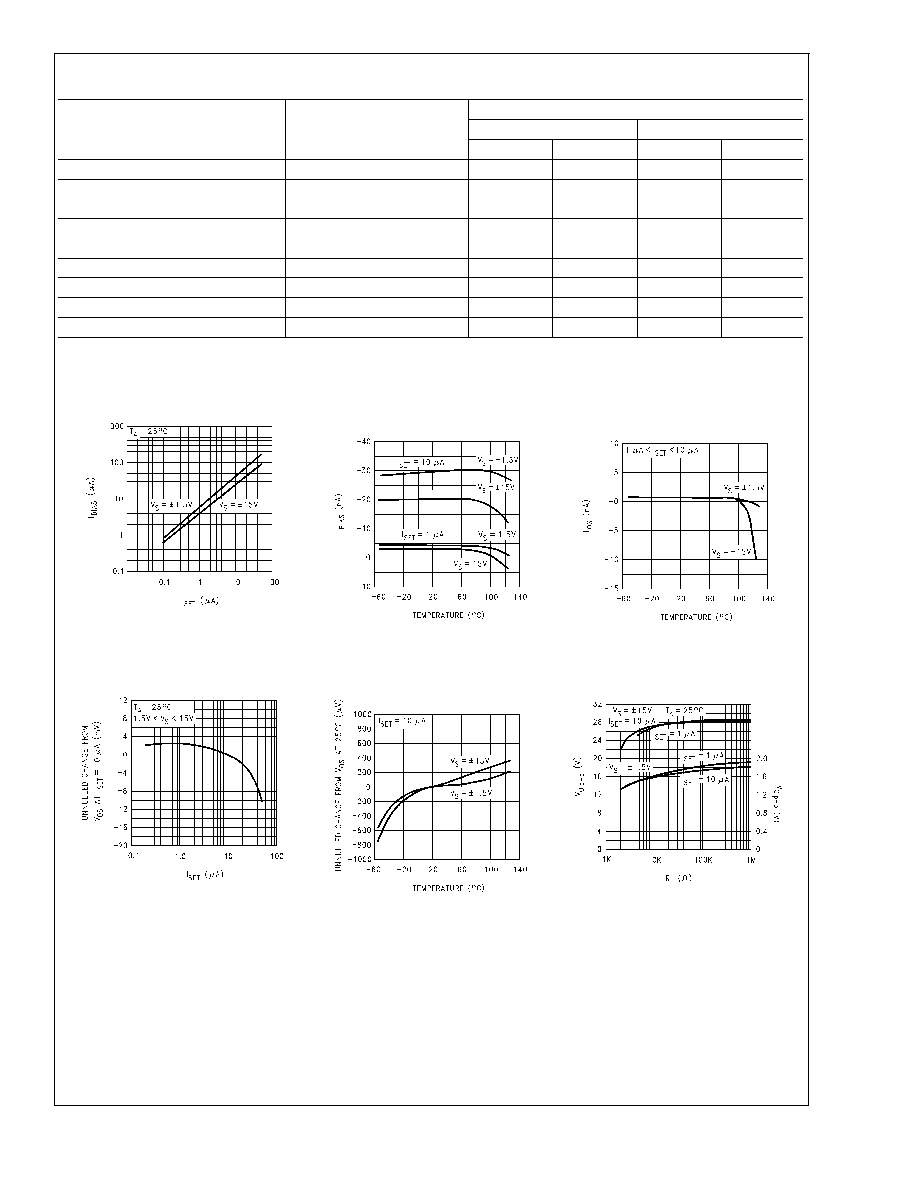
Typical Performance Characteristics
Input Bias Current vs I
SET
DS009300-15
Input Bias Current vs
Temperature
DS009300-16
Input Offset Current vs
Temperature
DS009300-17
Unnulled Input Offset Voltage
Change vs I
SET
DS009300-18
Unnulled Input Offset Voltage
Change vs Temperature
DS009300-19
Peak to Peak Output Voltage
Swing vs Load Resistance
DS009300-20
LM4250
www.national.com
5