LM431
Adjustable Precision Zener Shunt Regulator
General Description
The LM431 is a 3-terminal adjustable shunt regulator with
guaranteed temperature stability over the entire temperature
range of operation. It is now available in a chip sized pack-
age (4-Bump micro SMD) using National's micro SMD pack-
age technology. The output voltage may be set at any level
greater than 2.5V (V
REF
) up to 36V merely by selecting two
external resistors that act as a voltage divided network. Due
to the sharp turn-on characteristics this device is an excel-
lent replacement for many zener diode applications.
Features
n
Average temperature coefficient 50 ppm/∞C
n
Temperature compensated for operation over the full
temperature range
n
Programmable output voltage
n
Fast turn-on response
n
Low output noise
n
LM431 in micro SMD package
n
See AN-1112 for micro SMD considerations
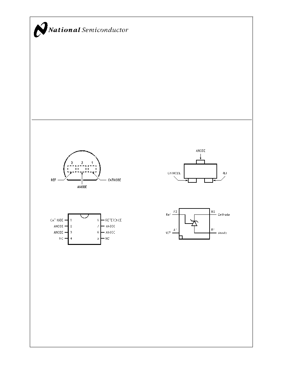
Connection Diagrams
Note:
*
NC = Not internally connected. Must be electrically isolated from the
rest of the circuit for the microSMD package.
TO-92: Plastic Package
DS010055-1
Top View
SO-8: 8-Pin Surface Mount
DS010055-2
Top view
SOT-23: 3-Lead Small Outline
DS010055-28
Top View
4-Bump micro SMD
DS010055-54
Top View
(bump side down)
March 2002
LM431
Adjustable
Precision
Zener
Shunt
Regulator
© 2002 National Semiconductor Corporation
DS010055
www.national.com

Ordering Information
Package
Typical Accuracy Order Number/Package Marking
Temperature
Range
Transport Media
NSC
Drawing
0.5%
1%
2%
TO-92
LM431CCZ/
LM431CCZ
LM431BCZ/
LM431BCZ
LM431ACZ/
LM431ACZ
0∞C to +70∞C
Rails
Z03A
LM431CIZ/
LM431CIZ
LM431BIZ/
LM431BIZ
LM431AIZ/
LM431AIZ
-40∞C to +85∞C
SO-8
LM431CCM/
431CCM
LM431BCM/
431BCM
LM431ACM/
LM431ACM
0∞C to +70∞C
Rails and Tape &Reel
M08A
LM431CIM/
431CIM
LM431BIM/
431BIM
LM431AIM/
LM431AIM
-40∞C to +85∞C
SOT-23
LM431CCM3/
N1B
LM431BCM3/
N1D
LM431ACM3/
N1F
0∞C to +70∞C
Rails and Tape &Reel
MF03A
LM431CIM3
N1A
LM431BIM3
N1C
LM431AIM3
N1E
-40∞C to +85∞C
micro SMD
≠
≠
LM431AIBP
LM431AIBPX(Note 1)
-40∞C to +85∞C
250 Units Tape and Reel
3k Units Tape and Reel
BPA04AFB
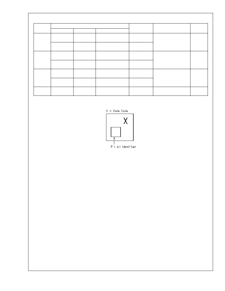
Note 1: The micro SMD package marking is a 1 digit manufacturing Date Code only
micro SMD Top View Marking Example
DS010055-56
LM431
www.national.com
2

Symbol and Functional Diagrams
DC Test Circuits
DS010055-99
DS010055-55
DS010055-4
FIGURE 1. Test Circuit for V
Z
= V
REF
DS010055-5
Note:
V
Z
= V
REF
(1 + R1/R2) + I
REF
∑
R1
FIGURE 2. Test Circuit for V
Z
>
V
REF
DS010055-6
FIGURE 3. Test Circuit for Off-State Current
LM431
www.national.com
3

Absolute Maximum Ratings
(Note 2)
If Military/Aerospace specified devices are required,
please contact the National Semiconductor Sales Office/
Distributors for availability and specifications.
Storage Temperature Range
-65∞C to +150∞C
Operating Temperature Range
Industrial (LM431xI)
-40∞C to +85∞C
Commercial (LM431xC)
0∞C to +70∞C
Soldering Information
Infrared or Convection (20 sec.)
235∞C
Wave Soldering (10 sec.)
260∞C (lead temp.)
Cathode Voltage
37V
Continuous Cathode Current
-10 mA to +150 mA
Reference Voltage
-0.5V
Reference Input Current
10 mA
Internal Power Dissipation (Notes 3, 4)
TO-92 Package
SO-8 Package
SOT-23 Package
0.78W
0.81W
0.28W
micro SMD Package
0.30W
Operating Conditions
Min
Max
Cathode Voltage
V
REF
37V
Cathode Current
1.0 mA
100 mA
LM431
Electrical Characteristics
T
A
= 25∞C unless otherwise specified
Symbol
Parameter
Conditions
Min
Typ
Max
Units
V
REF
Reference Voltage
V
Z
= V
REF
, I
I
= 10 mA
2.440
2.495
2.550
V
LM431A
(Figure 1 )
V
Z
= V
REF
, I
I
= 10 mA
2.470
2.495
2.520
V
LM431B
(Figure 1 )
V
Z
= V
REF
, I
I
= 10 mA
2.485
2.500
2.510
V
LM431C
(Figure 1 )
V
DEV
Deviation of Reference Input Voltage Over
V
Z
= V
REF
, I
I
= 10 mA,
8.0
17
mV
Temperature (Note 5)
T
A
= Full Range
(Figure 1 )
Ratio of the Change in Reference Voltage
I
Z
= 10 mA
V
Z
from V
REF
to 10V
-1.4
-2.7
mV/V
to the Change in Cathode Voltage
(Figure 2 )
V
Z
from 10V to 36V
-1.0
-2.0
I
REF
Reference Input Current
R
1
= 10 k
, R
2
=
,
2.0
4.0
µA
I
I
= 10 mA
(Figure 2 )
I
REF
Deviation of Reference Input Current over
R
1
= 10 k
, R
2
=
,
Temperature
I
I
= 10 mA,
0.4
1.2
µA
T
A
= Full Range
(Figure 2 )
I
Z(MIN)
Minimum Cathode Current for Regulation
V
Z
= V
REF
(Figure 1 )
0.4
1.0
mA
I
Z(OFF)
Off-State Current
V
Z
= 36V, V
REF
= 0V
(Figure 3 )
0.3
1.0
µA
r
Z
Dynamic Output Impedance (Note 6)
V
Z
= V
REF
, LM431A,
0.75
Frequency = 0 Hz
(Figure 1 )
V
Z
= V
REF
, LM431B, LM431C
0.50
Frequency = 0 Hz
(Figure 1 )
Note 2: Absolute Maximum Ratings indicate limits beyond which damage to the device may occur. Electrical specifications do not apply when operating the device
beyond its rated operating conditions.
Note 3: T
J Max
= 150∞C.
Note 4: Ratings apply to ambient temperature at 25∞C. Above this temperature, derate the TO-92 at 6.2 mW/∞C, the SO-8 at 6.5 mW/∞C, the SOT-23 at 2.2 mW/∞C
and the micro SMD at 3mW/∞C.
Note 5: Deviation of reference input voltage, V
DEV
, is defined as the maximum variation of the reference input voltage over the full temperature range.
LM431
www.national.com
4

LM431
Electrical Characteristics
(Continued)
Where:
T
2
- T
1
= full temperature change (0-70∞C).
V
REF
can be positive or negative depending on whether the slope is positive or negative.
Example: V
DEV
= 8.0 mV, V
REF
= 2495 mV, T
2
- T
1
= 70∞C, slope is positive.
Note 6: The dynamic output impedance, r
Z
, is defined as:
When the device is programmed with two external resistors, R1 and R2, (see
Figure 2
), the dynamic output impedance of the overall circuit, r
Z
, is defined as:
Equivalent Circuit
DS010055-7
The average temperature coefficient of the reference input voltage,
V
REF
, is defined as:
DS010055-3
LM431
www.national.com
5


