LM432
Dual Op Amp with On-Chip Fixed 2.5V Reference
General Description
The LM432 integrates two operational amplifiers and one
2.5V reference. The reference is based on the LMV431
adjustable shunt regulator with the output voltage adjusted
to a fixed 2.5V. The Op Amps are similar to the LM358 with
a common-mode input range that includes ground. Integrat-
ing the reference and Op Amps creates a solution for low
cost charging applications.
Applications
n
Low cost charging circuitry
n
Power supplies and adapters
Features
Dual Op Amp Circuitry
(Typical for V
S
= 5V)
n
Input offset voltage
0.6mV
n
Input offset current
1nA
n
Input bias current
3nA
n
Common-mode input voltage range
0V to V
S
-1V
n
Power supply current
150µA
Reference Circuitry
n
Reference voltage
2.5V
n
Reference voltage deviation (-40∞C to 85∞C)
4mV
n
Sink Current Capability
0.2mA to 10mA
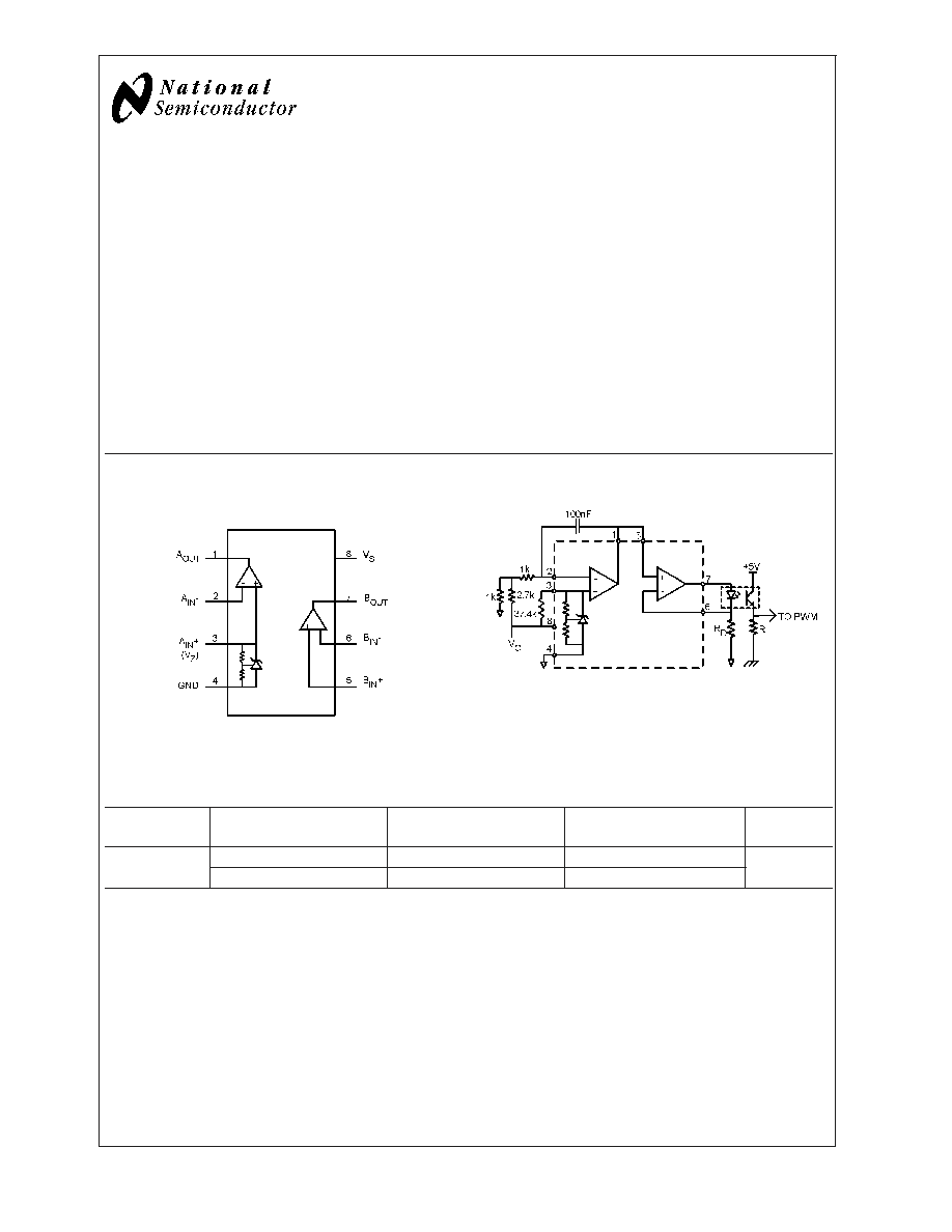
Connection Diagram
8-Pin SOIC
10139001
Top View
Application Circuit
10139002
Optocoupler Driver Circuit for Power Supply Isolation
Ordering Information
Package
Part Number
Package Marking
Transport Media
NSC
Drawing
8-Pin SOIC
LM432MA
LM432MA
Rails
M08A
LM432MAX
LM432MA
2.5k Unit Tape and Reel
July 2001
LM432
Dual
Op
Amp
with
On-Chip
Fixed
2.5V
Reference
© 2004 National Semiconductor Corporation
DS101390
www.national.com

Absolute Maximum Ratings
(Notes 1, 3)
If Military/Aerospace specified devices are required,
please contact the National Semiconductor Sales Office/
Distributors for availability and specifications.
Suppy Voltage (V
S
)
20V
Storage Temperature
-65∞C to 150∞C
Junction Temperature (T
J
)
150∞C
ESD Human Body Model
2kV
Input Voltage Range
-0.3V to 20V
Operating Ratings(Note 2),(Note 3)
Temperature Range
-40∞C to 85∞C
Supply Voltage (Note 8)
2.5V to 16V
Thermal Resistance(
JA
)
162∞C/W
Electrical Characteristics
The following specifications apply for both amplifiers at V
S
= 5V, V
CM
= 2.5V, V
O
= 2.5V, R
L
=
, and T
J
= 25∞C, unless other-
wise noted.
Symbol
Parameter
Conditions
Min
(Note 5)
Typ
(Note 4)
Max
(Note 5)
Units
OP Amp Circuitry
V
OS
Input Offset Voltage
Amplifier B only
-4
0.6
4
mV
I
OS
Input Offset Current
Amplifier B only
1
50
nA
I
B
Input Bias Current
Amplifier B only
3
150
nA
V
CM
Common-Mode Input Voltage Range
Amplifier B only,
CMRR
>
50dB
0
V
S
-1
V
I
S
Power Supply Current
Total for both amplifiers
150
500
µA
A
V
Voltage Gain
V
S
= 16V, 1V
<
V
O
<
11V,
R
L
= 10k
connected to V
S
/2
65
100
dB
V
OL
Output Voltage Low
2
50
mV
V
OH
Output Voltage High
V
S
≠ 1.5
V
S
≠ 1.3
V
I
SOURCE
Output Current Source
20
30
mA
I
SINK
Output Current Sink
5
11
mA
Reference Circuitry For Op Amp A The following specifications apply for I
Z
= 200µA and T
J
= 25∞C, unless otherwise noted.
V
Z
Reference Voltage at IN
+
Terminal
2.450
2.5
2.550
V
V
ZDEV
Reference Voltage Deviation at IN
+
Terminal Over Temperature
(Note 6),(Note 9)
-40∞C
T
J
85∞C
4
65
mV
I
Z (MIN)
Minimum Cathode Current for
Regulation at IN
+
(V
Z
) Terminal
150
200
µA
r
z
Dynamic Output Impedance (Note 7)
200µA
<
I
Z
<
1mA, Freq =
0Hz
0.2
Note 1: Absolute Maximum Ratings indicate limits beyond which damage to the device may occur.
Note 2: Operating Rating indicate conditions for which the device is functional. These rating do not guarantee specific performance limits. For guaranteed
specifications and test conditions, see the Electrical Characteristics. The guaranteed specifications apply only for the test conditions listed. Some performance
characteristics may degrade when the device is not operated under the listed test conditions.
Note 3: All voltages are measured with respect to GND = 0V
DC
, unless otherwise specified.
Note 4: Typicals represent the most likely parametic norm.
Note 5: Guaranteed to National's Average Outgoing Quality Level (AOQL).
Note 6: Reference voltage deviation, V
ZDEV
, is defined as the maximum variation of the reference input voltage over the full temperature range.
Note 7: The Dynamic Output Impendance, r
z
, is defined as r
z
=
V
Z
/
I
Z
.
Note 8: Minimum value of operating voltage is for Amplifier B only.
Note 9: Typical Temperature drift
V/T = 12.8ppm/∞C
LM432
www.national.com
2

Physical Dimensions
inches (millimeters)
unless otherwise noted
8-Pin SOIC
NS Package Number M08A
LIFE SUPPORT POLICY
NATIONAL'S PRODUCTS ARE NOT AUTHORIZED FOR USE AS CRITICAL COMPONENTS IN LIFE SUPPORT
DEVICES OR SYSTEMS WITHOUT THE EXPRESS WRITTEN APPROVAL OF THE PRESIDENT AND GENERAL
COUNSEL OF NATIONAL SEMICONDUCTOR CORPORATION. As used herein:
1. Life support devices or systems are devices or
systems which, (a) are intended for surgical implant
into the body, or (b) support or sustain life, and
whose failure to perform when properly used in
accordance with instructions for use provided in the
labeling, can be reasonably expected to result in a
significant injury to the user.
2. A critical component is any component of a life
support device or system whose failure to perform
can be reasonably expected to cause the failure of
the life support device or system, or to affect its
safety or effectiveness.
BANNED SUBSTANCE COMPLIANCE
National Semiconductor certifies that the products and packing materials meet the provisions of the Customer Products
Stewardship Specification (CSP-9-111C2) and the Banned Substances and Materials of Interest Specification
(CSP-9-111S2) and contain no ``Banned Substances'' as defined in CSP-9-111S2.
National Semiconductor
Americas Customer
Support Center
Email: new.feedback@nsc.com
Tel: 1-800-272-9959
National Semiconductor
Europe Customer Support Center
Fax: +49 (0) 180-530 85 86
Email: europe.support@nsc.com
Deutsch Tel: +49 (0) 69 9508 6208
English
Tel: +44 (0) 870 24 0 2171
FranÁais Tel: +33 (0) 1 41 91 8790
National Semiconductor
Asia Pacific Customer
Support Center
Email: ap.support@nsc.com
National Semiconductor
Japan Customer Support Center
Fax: 81-3-5639-7507
Email: jpn.feedback@nsc.com
Tel: 81-3-5639-7560
www.national.com
LM432
Dual
Op
Amp
with
On-Chip
Fixed
2.5V
Reference
National does not assume any responsibility for use of any circuitry described, no circuit patent licenses are implied and National reserves the right at any time without notice to change said circuitry and specifications.