LM4431
Micropower Shunt Voltage Reference
General Description
Ideal for space critical applications, the LM4431 voltage ref-
erence is available in the sub-miniature (3 mm x 1.3 mm)
SOT-23 surface-mount package. The LM4431's advanced
design eliminates the need for an external stabilizing capaci-
tor while ensuring stability with any capacitive load, thus
making the LM4431 easy to use. The operating current
range is 100 µA to 15 mA.
The LM4431 utilizes fuse and zener-zap reverse breakdown
voltage trim during wafer sort to ensure that the parts have
an accuracy of better than
±
2.0% at 25∞C. Bandgap refer-
ence temperature drift curvature correction and low dynamic
impedance ensure stable reverse breakdown voltage accu-
racy over a wide range of operating temperatures and cur-
rents.
Features
n
Small package: SOT-23
n
No output capacitor required
n
Tolerates capacitive loads
n
Fixed reverse breakdown voltage of 2.50V
Key Specifications
n
Output voltage tolerance 25∞C:
±
2.0% (max)
n
Low output noise (10 Hz to 10 kHz): 35 µV
rms
(typ)
n
Wide operating current range: 100 µA to 15 mA
n
Commercial temperature range: 0∞C to +70∞C
n
Low temperature coefficient: 30 ppm/∞C (typ)
Applications
n
Portable, Battery-Powered Equipment
n
Data Acquisition Systems
n
Instrumentation
n
Process Control
n
Energy Management
n
Product Testing
n
Power Supplies
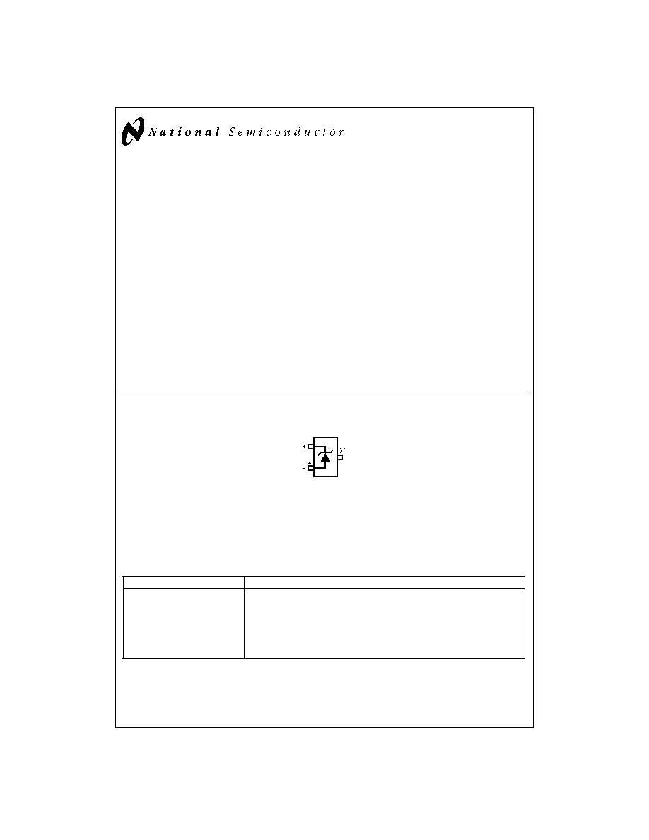
Connection Diagram
SOT-23 Package Marking Information
Only three fields of marking are possible on the SOT-23's small surface. The following table gives the meaning of the three
fields.
Part Marking
Field Definition
S2E
First Field:
S = Reference
Second Field:
2 = 2.500V Voltage Option
Third Field:
E = Initial Reverse Breakdown Voltage Tolerance of
±
2.0%
SOT-23
DS011374-1
* This pin must be left floating or connected to pin 2.
Top View
Order Number LM4431M3-2.5
See NS Package Number M03B
(JEDEC Registration TO-236AB)
July 1998
LM4431
Micropower
Shunt
V
oltage
Reference
© 1998 National Semiconductor Corporation
DS011374
www.national.com

Absolute Maximum Ratings
(Note 1)
If Military/Aerospace specified devices are required,
please contact the National Semiconductor Sales Office/
Distributors for availability and specifications.
Reverse Current
20 mA
Forward Current
10 mA
Power Dissipation (T
A
= 25∞C) (Note 2)
M3 Package
306 mW
Storage Temperature
-65∞C to +150∞C
Lead Temperature
M3 Package
Vapor phase (60 seconds)
+215∞C
Infrared (15 seconds)
+220∞C
ESD Susceptibility
Human Body Model (Note 3)
2 kV
Machine Model (Note 3)
200V
See AN-450 "Surface Mounting Methods and Their Effect
on Product Reliability" for other methods of soldering
surface mount devices.
Operating Ratings
(Notes 1, 2)
Temperature Range
(T
min
T
A
T
max
)
0∞C
T
A
+70∞C
Reverse Current
LM4431-2.5
100 µA to 15 mA
LM4431-2.5
Electrical Characteristics
Boldface limits apply for T
A
= T
J
= T
MIN
to T
MAX
; all other limits T
A
= T
J
= 25∞C.
Symbol
Parameter
Conditions
Typical
LM4431M3
Units
(Note 4)
Limits
(Limit)
(Note 5)
V
R
Reverse Breakdown Voltage
I
R
= 100 µA
2.500
V
Reverse Breakdown
VoltageTolerance
I
R
= 100 µA
±
50
mV (max)
I
RMIN
Minimum Operating Current
45
µA
100
µA (max)
V
R
/
T
Average Reverse Breakdown
I
R
= 10 mA
±
30
ppm/∞C
Voltage Temperature
I
R
= 1 mA
±
30
ppm/∞C
Coefficient
I
R
= 100 µA
±
30
ppm/∞C
V
R
/
I
R
Reverse Breakdown Voltage
I
RMIN
I
R
1 mA
0.4
mV
Change with Operating
1.0
mV (max)
Current Change
1.2
mV (max)
1 mA
I
R
15 mA
2.5
mV
8.0
mV (max)
25
mV (max)
Z
R
Reverse Dynamic Impedance
I
R
= 1 mA, f = 120 Hz
1.0
I
AC
= 0.1 I
R
e
N
Wideband Noise
I
R
= 100 µA
35
µV
rms
10 Hz
f
10 kHz
V
R
Reverse Breakdown Voltage
t = 1000 hrs
Long Term Stability
T = 25∞C
±
0.1∞C
120
ppm
I
R
= 100 µA
Note 1: Absolute Maximum Ratings indicate limits beyond which damage to the device may occur. Operating Ratings indicate conditions for which the device is func-
tional, but do not guarantee specific performance limits. For guaranteed specifications and test conditions, see the Electrical Characteristics. The guaranteed speci-
fications apply only for the test conditions listed. Some performance characteristics may degrade when the device is not operated under the listed test conditions.
Note 2: The maximum power dissipation must be derated at elevated temperatures and is dictated by T
Jmax
(maximum junction temperature),
JA
(junction to am-
bient thermal resistance), and T
A
(ambient temperature). The maximum allowable power dissipation at any temperature is PD
max
= (T
Jmax
- T
A
)/
JA
or the number
given in the Absolute Maximum Ratings, whichever is lower. For the LM4431, T
Jmax
= 125∞C, and the typical thermal resistance (
JA
), when board mounted, is
326∞C/W for the SOT-23 package.
Note 3: The human body model is a 100 pF capacitor discharged through a 1.5 k
resistor into each pin. The machine model is a 200 pF capacitor discharged di-
rectly into each pin.
Note 4: Typicals are at T
J
= 25∞C and represent most likely parametric norm.
Note 5: Limits are 100% production tested at 25∞C. Limits over temperature are guaranteed through correlation using Statistical Quality Control (SQC) methods. The
limits are used to calculate National's AOQL.
www.national.com
2
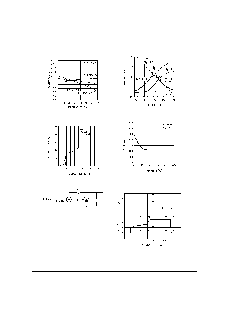
Typical Performance Characteristics
Start-Up Characteristics
Temperature Drift for Different
Average Temperature Coefficient
DS011374-2
Output Impedance vs Frequency
DS011374-3
Reverse Characteristics and
Minimum Operating Current
DS011374-4
Noise Voltage
DS011374-5
DS011374-6
LM4431-2.5
R
S
= 30k
DS011374-7
3
www.national.com
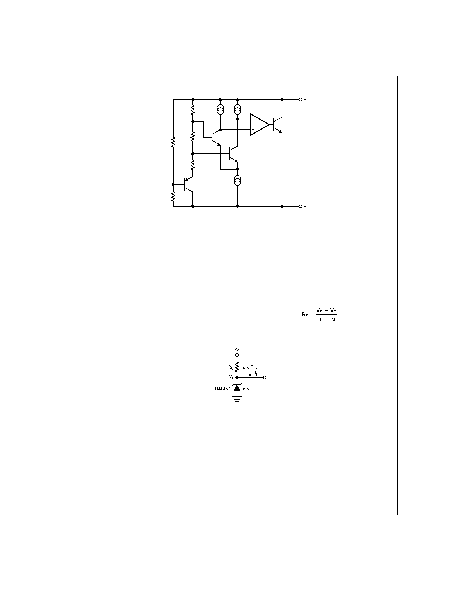
Functional Block Diagram
Applications Information
The LM4431 is a micro-power curvature-corrected 2.5V
bandgap shunt voltage reference. For space critical applica-
tions, the LM4431 is available in the sub-miniature SOT-23
surface-mount package. The LM4431 has been designed for
stable operation without the need of an external capacitor
connected between the "+" pin and the "-" pin. If, however, a
bypass capacitor is used, the LM4431 remains stable. The
operating current range is 100 µA to 15 mA.
The LM4431's SOT-23 package has a parasitic Schottky di-
ode between pin 2 (-) and pin 3 (Die attach interface con-
tact). Therefore, pin 3 of the SOT-23 package must be left
floating or connected to pin 2.
In a conventional shunt regulator application (
Figure 1) , an
external series resistor (R
S
) is connected between the sup-
ply voltage and the LM4431. R
S
determines the current that
flows through the load (I
L
) and the LM4431 (I
Q
). Since load
current and supply voltage may vary, R
S
should be small
enough to supply at least the minimum acceptable I
Q
to the
LM4431 even when the supply voltage is at its minimum and
the load current is at its maximum value. When the supply
voltage is at its maximum and I
L
is at its minimum, R
S
should
be large enough so that the current flowing through the
LM4431 is less than 15 mA.
R
S
is determined by the supply voltage, (V
S
), the load and
operating current, (I
L
and I
Q
), and the LM4431's reverse
breakdown voltage, V
R
.
Typical Applications
DS011374-8
DS011374-9
FIGURE 1. Shunt Regulator
www.national.com
4
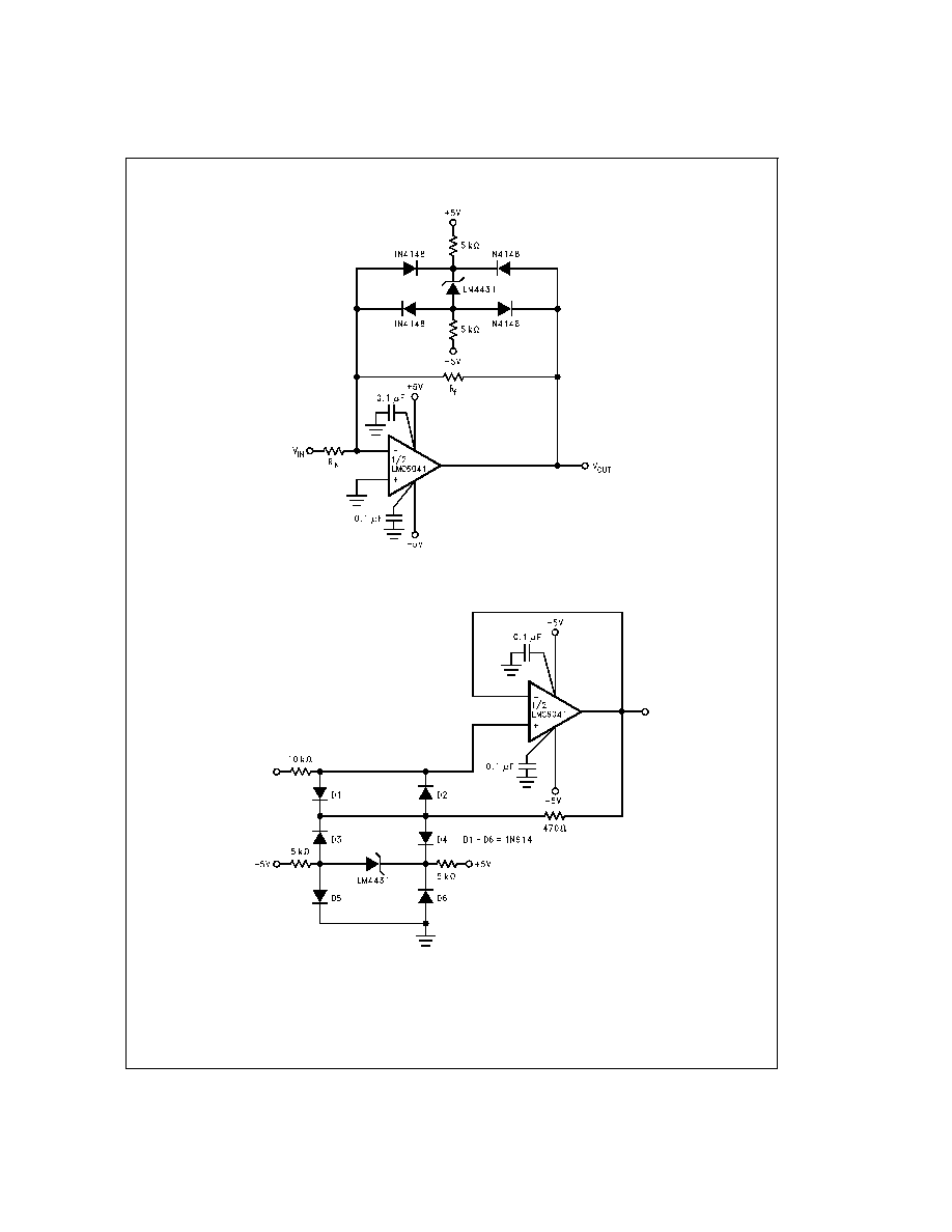
Typical Applications
(Continued)
DS011374-10
FIGURE 2. Bounded amplifier reduces saturation-induced delays and can prevent succeeding stage damage.
Nominal clamping voltage is
±
3.9V (LM4431's reverse breakdown voltage +2 diode V
F
).
DS011374-11
FIGURE 3. Protecting Op Amp input. The bounding voltage is
±
4V with the LM4431
(LM4431's reverse breakdown voltage + 3 diode V
F
).
5
www.national.com