 | –≠–ª–µ–∫—Ç—Ä–æ–Ω–Ω—ã–π –∫–æ–º–ø–æ–Ω–µ–Ω—Ç: LM4540 | –°–∫–∞—á–∞—Ç—å:  PDF PDF  ZIP ZIP |
LM4540
AC '97 Codec with National 3D Sound
General Description
The LM4540 is an audio codec for PC systems which per-
forms the analog-intensive function of the Analog Codec '97
Rev 1.03 architecture. Using 18-Bit
A/D and D/A convert-
ers, the LM4540 provides 90dB of dynamic range.
The LM4540 was designed specifically to provide a high
quality audio path and provide all analog functionality in a PC
audio system. It features full duplex stereo A/D's and D/A's
and an analog mixer with 2 stereo and 3 mono inputs, each
of which has separate gain, attenuation and mute control. In
addition, the LM4540 provides National's 3D Sound stereo
enhancement technology.
The LM4540 features AC-Link, a synchronous, fixed rate se-
rial bus for connection to the digital AC '97 Controller. The
separation of the analog and digital functions of the AC '97
architecture allows for system design flexibility and in-
creased overall performance.
Key Specifications
n
Analog Mixer Dynamic Range
95dB (typ)
n
D/A Dynamic Range
89dB (typ)
n
A/D Dynamic Range
90dB (typ)
Features
n
Audio Codec '97 compliant
n
Stereo 18-Bit
A/D's and D/A's with 128X
oversampling
n
National's 3D Sound circuitry
n
Power management support
n
Digital Interface 3V and 5V compliant
Applications
n
PC Audio Systems Requiring Only 2 Stereo Inputs (CD,
Line) and 3 Mono Inputs (Mic, Phone, PC Beep)
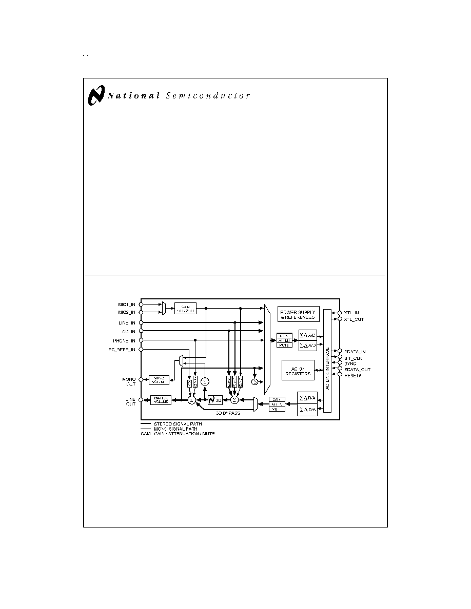
Block Diagram
DS100906-1
FIGURE 1. LM4540 Block Diagram
February 1999
LM4540
AC
'97
Codec
with
National
3D
Sound
© 1999 National Semiconductor Corporation
DS100906
www.national.com
Absolute Maximum Ratings
(Note 3)
If Military/Aerospace specified devices are required,
please contact the National Semiconductor Sales Office/
Distributors for availability and specifications.
Supply Voltage
6.0V
Storage Temperature
-65∞C to +150∞C
Input Voltage
-0.3V to V
DD
+0.3V
ESD Susceptibility (Note 5)
2500V
pins 27, 28
1500V
pin 3
750V
ESD Susceptibility (Note 6)
200V
pin 3
100V
Junction Temperature
150∞C
Soldering Information
TQFP Package
Vapor Phase (60 sec.)
215∞C
Infrared (15 sec.)
220∞C
See AN-450
Surface Mounting and their Effects on
Product Reliability
for other methods of
soldering surface mount devices.
JA
(typ) -- VBH48A
74∞C/W
Operating Ratings
Temperature Range
T
MIN
T
A
T
MAX
-40∞C
T
A
85∞C
Analog Supply Range
4.2V
AV
DD
5.5V
Digital Supply Range
3.0V
DV
DD
5.5V
Electrical Characteristics
(Notes 1, 3)
The following specifications apply for AV
DD
= 5V, DV
DD
= 5V unless otherwise noted. Limits apply for T
A
= 25∞C. The reference
for 0dB is 1Vrms unless otherwise specified.
Symbol
Parameter
Conditions
LM4540
Units
(Limits)
Typical
(Note 7)
Limit
(Note 8)
AV
DD
Analog Supply Range
4.2
V (min)
5.5
V (max)
DV
DD
Digital Supply Range
3.0
V (min)
5.5
V (max)
I
DDD
Digital Quiescent Power Supply
Current
D
VDD
= 5V
38
mA
D
VDD
= 3.3V
20
mA
I
DDA
Analog Quiescent Power Supply
Current
55
mA
I
SD
Shutdown Current
1.5
mA
V
REF
Reference Voltage
2.23
V
PSRR
Power Supply Rejection Ratio
40
dB
Analog Loopthru Mode
Dynamic Range (Note 2)
CD Input to Line Output, -60dB Input
THD+N, A-Weighted
95
90
dB (min)
THD
Total Harmonic Distortion
V
O
= -3dB, f = 1kHz, R
L
= 10k
0.01
0.02
% (max)
Analog Input Section
V
IN
Line Input Voltage
1
Vrms
Mic Input with 20dB Gain
0.1
Vrms
Mic Input with 0dB Gain
1
Vrms
Xtalk
Crosstalk
CD Left to Right
-85
-70
dB (max)
Z
IN
Input Impedance
40
10
k
(min)
C
IN
Input Capacitance
15
pF
Interchannel Gain Mismatch
CD Left to Right
0.04
dB
Record Gain Amplifier - A/D
A
S
Step Size
0dB to 22.5dB
1.5
dB
Mixer Section
A
S
Step Size
+12dB to -34.5dB
1.5
dB
A
M
Mute Attenuation
86
dB
Analog to Digital Converters
Resolution
18
Bits
www.national.com
2
Electrical Characteristics
(Notes 1, 3) (Continued)
The following specifications apply for AV
DD
= 5V, DV
DD
= 5V unless otherwise noted. Limits apply for T
A
= 25∞C. The reference
for 0dB is 1Vrms unless otherwise specified.
Symbol
Parameter
Conditions
LM4540
Units
(Limits)
Typical
(Note 7)
Limit
(Note 8)
Analog to Digital Converters
Dynamic Range (Note 2)
-60dB Input THD+N, A-Weighted
90
75
dB (min)
Frequency Response
-1dB Bandwidth
20
kHz
Digital to Analog Converters
Resolution
18
Bits
Dynamic Range (Note 2)
-60dB Input THD+N, A-Weighted
89
85
dB (min)
THD
Total Harmonic Distortion
V
IN
= -3dB, f=1kHz, R
L
= 10k
0.01
0.03
% (max)
Frequency Response
-1dB Bandwidth
21
kHz
Group Delay (Note 2)
1
mS (max)
Out of Band Energy
-40
dB
Stop Band Rejection
70
dB
D
T
Discrete Tones
-96
dB
Output Volume Section
A
S
Step Size
0dB to -46.5dB
1.5
dB
A
M
Mute Attenuation
86
dB
Digital I/O (Note 2)
V
IL
Low level input voltage
0.30 x
DVDD
V (max)
V
HI
High level input voltage
0.40 x
DVDD
V (min)
V
OH
High level output voltage
0.50 x
DVDD
V (min)
V
OL
Low level output voltage
0.20 x
DVDD
V (max)
I
L
Input Leakage Current
AC Link inputs
±
10
µA (max)
I
L
Tri state Leakage Current
High impedance AC Link outputs
±
10
µA (max)
I
DR
Output drive current
AC Link outputs
5
mA
Digital Timing Specifications (Note 2)
F
BC
BIT_CLK frequency
12.288
MHz
T
BCP
BIT_CLK period
81.4
nS
T
CH
BIT_CLK high
Variation of BIT_CLK period from 50%
duty cycle
±
20
% (max)
F
SYNC
SYNC frequency
48
kHz
T
SP
SYNC period
20.8
µS
T
SH
SYNC high pulse width
1.3
µS
T
SL
SYNC low pulse width
19.5
µS
T
SETUP
Setup Time
SDATA_IN, SDATA_OUT to falling
edge of BIT_CLK
15
nS (min)
T
HOLD
Hold Time
Hold time of SDATA_IN, SDATA_OUT
from falling edge of BIT_CLK
5
nS (min)
T
RISE
Rise Time
BIT_CLK, SYNC, SDATA_IN or
SDATA_OUT
6
nS (max)
T
FALL
Fall Time
BIT_CLK, SYNC, SDATA_IN or
SDATA_OUT
6
nS (max)
T
RST_LOW
RESET# active low pulse width
For cold reset
1.0
µS (min)
T
RST2CLK
RESET# inactive to BIT_CLK start
up
For cold reset
162.8
nS (min)
www.national.com
3
Electrical Characteristics
(Notes 1, 3) (Continued)
The following specifications apply for AV
DD
= 5V, DV
DD
= 5V unless otherwise noted. Limits apply for T
A
= 25∞C. The reference
for 0dB is 1Vrms unless otherwise specified.
Symbol
Parameter
Conditions
LM4540
Units
(Limits)
Typical
(Note 7)
Limit
(Note 8)
Digital Timing Specifications (Note 2)
T
SH
SYNC active high pulse width
For warm reset
1.3
µS
T
SYNC2CLK
SYNC inactive to BIT_CLK start up
For warm reset
162.8
nS (min)
T
SU2RST
Setup to trailing edge of RESET#
For ATE Test Mode
15
nS (min)
T
RST2HZ
Rising edge of RESET# to Hi-Z
For ATE Test Mode
25
nS (max)
Note 1: All voltages are measured with respect to the ground pin, unless otherwise specified.
Note 2: These specifications are guaranteed by design and characterization; they are not production tested.
Note 3:
Absolute Maximum Ratings indicate limits beyond which damage to the device may occur. Operating Ratings indicate conditions for which the device is func-
tional, but do not guarantee specific performance limits.
Electrical Characteristics state DC and AC electrical specifications under particular test conditions which guar-
antee specific performance limits. This assumes that the device is within the Operating Ratings. Specifications are not guaranteed for parameters where no limit is
given, however, the typical value is a good indication of device performance.
Note 4: The maximum power dissipation must be derated at elevated temperatures and is dictated by T
JMAX
,
JA
, and the ambient temperature T
A
. The maximum
allowable power dissipation is P
DMAX
= (T
JMAX
≠T
A
)/
JA
or the number given in Absolute Maximum Ratings, whichever is lower. For the LM4540, T
JMAX
= 150∞C. The
typical junction-to-ambient thermal resistance is 74∞C/W for package number VBH48A.
Note 5: Human body model, 100 pF discharged through a 1.5 k
resistor.
Note 6: Machine Model, 220 pF≠240 pF discharged through all pins.
Note 7: Typicals are measured at 25∞C and represent the parametric norm.
Note 8: Limits are guaranteed to National's AOQL (Average Outgoing Quality Level).
www.national.com
4
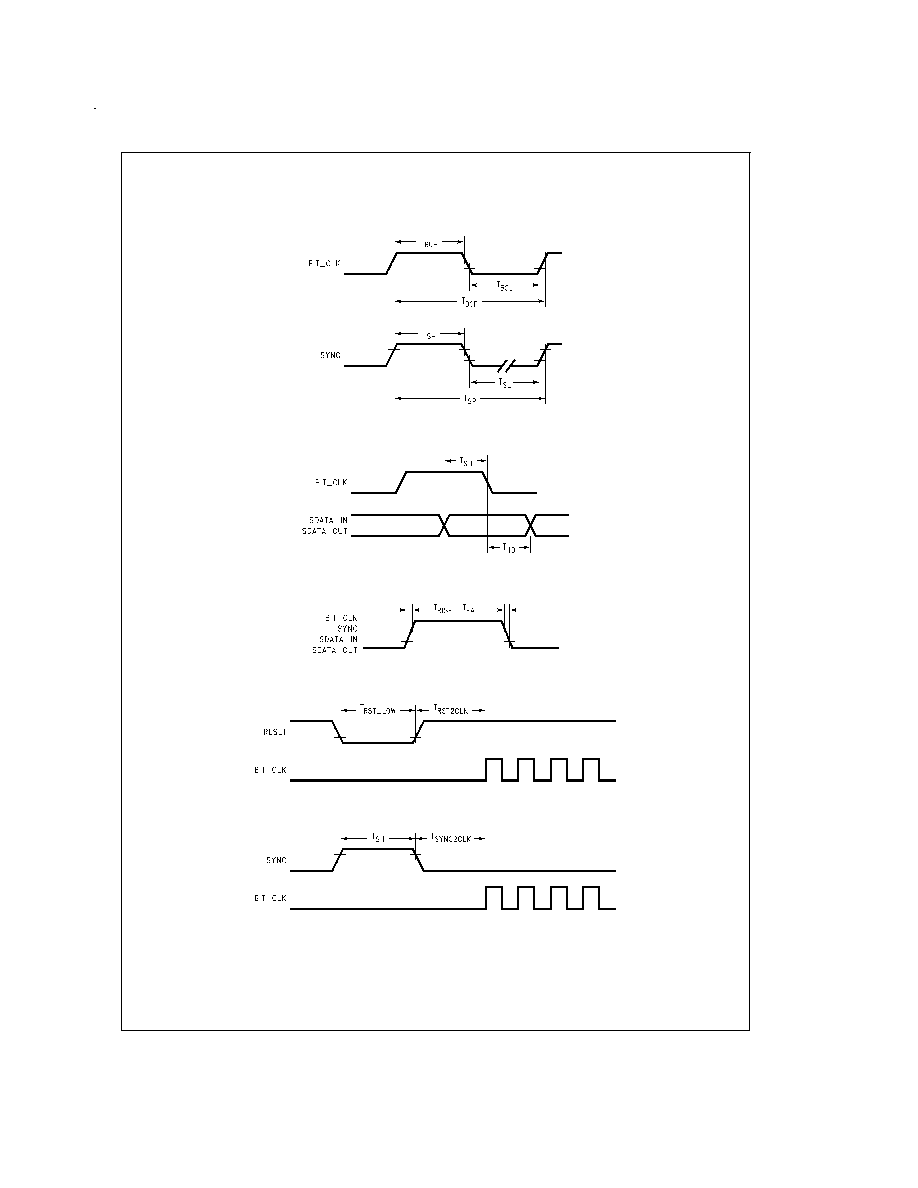
Timing Diagrams
Clocks
DS100906-10
Data Setup and Hold
DS100906-11
Digital Rise and Fall
DS100906-12
Cold Reset
DS100906-13
Warm Reset
DS100906-14
www.national.com
5