LM4663
2 Watt Stereo Class D Audio Power Amplifier with Stereo
Headphone Amplifier
General Description
The LM4663 is a fully integrated single supply, high effi-
ciency Class D audio power amplifier solution. The LM4663
utilizes a continuous time delta-sigma modulation technique
that lowers output noise and THD when compared to con-
ventional pulse width modulators.
The LM4663 also features a stereo headphone amplifier that
delivers 80mW into a 32
headset with less than 0.5% THD.
The LM4663 has two stereo inputs that can be selected to
drive either the headphone amplifier or the Class D amplifier.
All amplifiers are protected with thermal shutdown.
In standby mode, the LM4663 draws an extremely low 2�A
supply current. With a 4
load, the IC's efficiency for a
250mW power level is 69%, reaching 83% at a power level
of 2W. The IC features click and pop reduction circuitry that
minimizes audible popping during device turn-on and
turn-off. The LM4663 is available in a 24-lead TSSOP pack-
age, ideal for portable and desktop computer applications.
Key Specifications
n
P
O
at THD+N=1%
2.1W (typ)
n
THD+N at 1kHz at 1 Watt into 4
(Power
Amp)
0.2% (typ)
n
Efficiency at 2 Watt into 4
83% (typ)
n
Efficiency at 250mW into 4
69% (typ)
n
Total quiescent power supply current
22mA (typ)
n
Total shutdown power supply current
2�A (typ)
n
THD+N 1kHz, 20mW, 32
(Headphone)
0.15% (typ)
n
Single supply range
4.5V to 5.5V
Features
n
Delta-sigma modulator.
n
Two stereo input selector.
n
"Click and pop" suppression circuitry.
n
Micropower shutdown mode.
n
24 lead TSSOP package (No heatsink required).
n
Stereo headphone amplifier.
Applications
n
Portable computers
n
Desktop computers
n
Multimedia Monitors
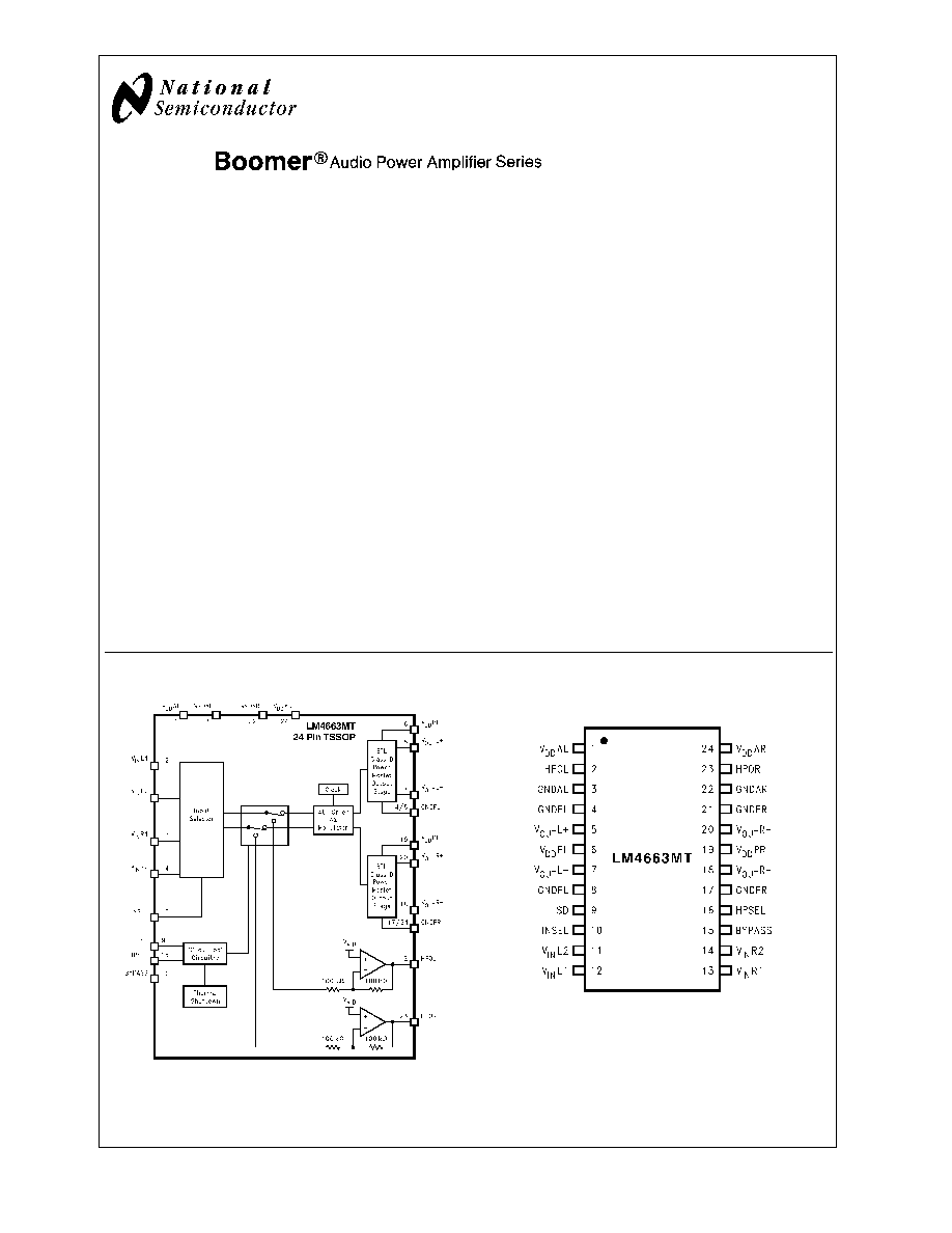
Block Diagram
10126901
Connection Diagram
TSSOP Package
10126902
Top View
Order Number LM4663MT
See NS Package Number MTC24
(TSSOP Package)
BOOMER
TM
is a trademark of National Semiconductor Corporation.
November 2002
LM4663
2
W
att
Stereo
Class
D
Audio
Power
Amplifier
with
Stereo
Headphone
Amplifier
� 2002 National Semiconductor Corporation
DS101269
www.national.com
Absolute Maximum Ratings
(Note 2)
If Military/Aerospace specified devices are required,
please contact the National Semiconductor Sales Office/
Distributors for availability and specifications.
Supply Voltage
6.0V
Input Voltage
-0.3V to V
DD
+0.3V
Power Dissipation (Note 3)
Internally Limited
Load Resistance
2.5
, min
ESD Susceptibility(Note 4)
2000V
Pins 5,7,18,20
600V
ESD Susceptibility (Note 5)
200V
Pins 5,7,18,20
50V
Junction Temperature (Note 6)
150�C
Storage Temperature
-65�C
T
A
150�C
Soldering Information
TSSOP Package
Vapor Phase (60 sec.)
215�C
Infrared (15 sec.)
220�C
See AN-450 "Surface Mounting and their Effects on
Product Reliability" for other methods of soldering surface
mount devices.
Operating Ratings
(Notes 1, 2)
Temperature Range
T
MIN
T
A
T
MAX
-40�C
T
A
+85�C
Supply Voltage
4.5V
V
DD
5.5V
Thermal Resistance (TSSOP Package)
JA
80�C/W
JC
20�C/W
Electrical Characteristics
(Notes 1, 2, 7)
The following specifications apply for V
DD
= 5V, R
L
= 4
, LC filter values as shown in Figure 1, unless otherwise specified.
Limits apply for T
A
= 25�C.
Symbol
Parameter
Conditions
LM4663
Units
Typical
Max
Min
V
S
Operating Supply Voltage Range
5
5.5
4.5
V
I
S
Quiescent Power Supply Current,
Class D Mode
V
IN
= 0V
RMS
, V
HPSEL
= 0V
22
35
mA
I
S
Quiescent Power Supply Current,
Headphone Mode
V
IN
= 0V
RMS
, V
HPSEL
= V
S
5
10
mA
I
SD
Quiescent Power Supply Current,
Shutdown Mode
V
SD
= 5V
2
�A
R
IN
Input Resistance in Both Modes
20
k
V
IH
Minimum High Level Input
Voltage
Shutdown Pin & Input Select Pin
4.5
V
V
IL
Maximum Low Level Input
Voltage
Shutdown Pin & Input Select Pin
0.5
V
V
IH
Minimum High Level Input
Voltage
Headphone Select Pin
4.5
V
V
IL
Maximum Low Level Input
Voltage
Headphone Select Pin
0.5
V
Power Amplifiers
P
O
R
Output Power, Per Channel
THD+N
1%, f
IN
= 1kHz
2.1
W
P
D1
Power Dissipation
P
O
= 2W/Chan, f
IN
= 1kHz
0.82
W
P
D2
Power Dissipation
P
O
= 1W/Chan, f
IN
= 1kHz
0.49
W
P
D3
Power Dissipation
P
O
= .25W/Chan, f
IN
= 1kHz
0.23
W
E
FF1
Efficiency
P
O
= 2W/Chan, f
IN
= 1kHz
83
%
E
FF2
Efficiency
P
O
= 1W/Chan, R
L
= 8
, f
IN
=
1kHz
85
80
%
E
FF3
Efficiency
P
O
= .25W/Chan, f
IN
= 1kHz
69
%
THD+N
Harmonic Distortion + Noise
P
O
= 1W/Chan, f
IN
= 1kHz
0.2
%
V
NOISE
Output Noise Voltage, RMS.
A-Weighted
R
SOURCE
= 50
, C
IN
= 1�F, BW
= 8Hz to 22kHz
200
�V
PSRR
Power Supply Rejection Ratio
(Referred to Input)
200mV, 1kHz, V
IN
= 0
44
dB
LM4663
www.national.com
2
Electrical Characteristics
(Notes 1, 2, 7) (Continued)
The following specifications apply for V
DD
= 5V, R
L
= 4
, LC filter values as shown in Figure 1, unless otherwise specified.
Limits apply for T
A
= 25�C.
Symbol
Parameter
Conditions
LM4663
Units
Typical
Max
Min
A
V
Voltage Gain
1kHz, V
IN
= 100mV, R
L
= 4
13
dB
A
V
L-A
V
R
Stereo Gain Tracking
1kHz, V
IN
= 100mV, R
L
= 4
0.1
dB
Headphone Amplifiers
P
O
Power Out Per Channel
THD+N
1%, R
L
= 32
, f
IN
=
1kHz
80
60
mW
THD+N
Distortion + Noise
P
O
= 20mW, R
L
= 32
, f
IN
=
1kHz
0.15
%
V
NOISE
Output Noise Voltage, RMS
R
IN
= 50
, C
IN
= 1�F, BW =
8Hz to 22kHz
30
�V
PSRR
Power Supply Rejection Ratio
(Referred to Input)
200mV, 1kHz, V
IN
= 0, R
L
=
32
44
dB
A
V
Voltage Gain
1kHz, V
IN
= 100mV, R
L
= 32
5.5
dB
A
V
L-A
V
R
Stereo Gain Tracking
1kHz, V
IN
= 100mV, R
L
= 32
0.1
dB
Note 1: All voltages are measured with respect to the ground pin, unless otherwise specified.
Note 2: "Absolute Maximum Ratings" indicate limits beyond which damage to the device may occur. "Operating Ratings" indicate conditions for which the device
is functional, but do not guarantee specific performance limits. "Electrical Characteristics" state DC and AC electrical specifications under particular test conditions
which guarantee specific performance limits. This assumes that the device is within the Operating Ratings. Specifications are not guaranteed for parameters where
no limit is given, however, the typical value is a good indication of device performance.
Note 3: For operating at case temperatures above 25�C, the device must be derated based on a 150�C maximum junction temperature and a thermal resistance
of
JA
= 80�C/W (junction to ambient).
Note 4: Human body model, 100 pF discharged through a 1.5 k
resistor.
Note 5: Machine Model 220pF-240pF discharged through all pins.
Note 6: The operating junction temperature maximum is 150�C.
Note 7: Limits are guaranteed to National's AOQL (Average Outgoing Quality Level).
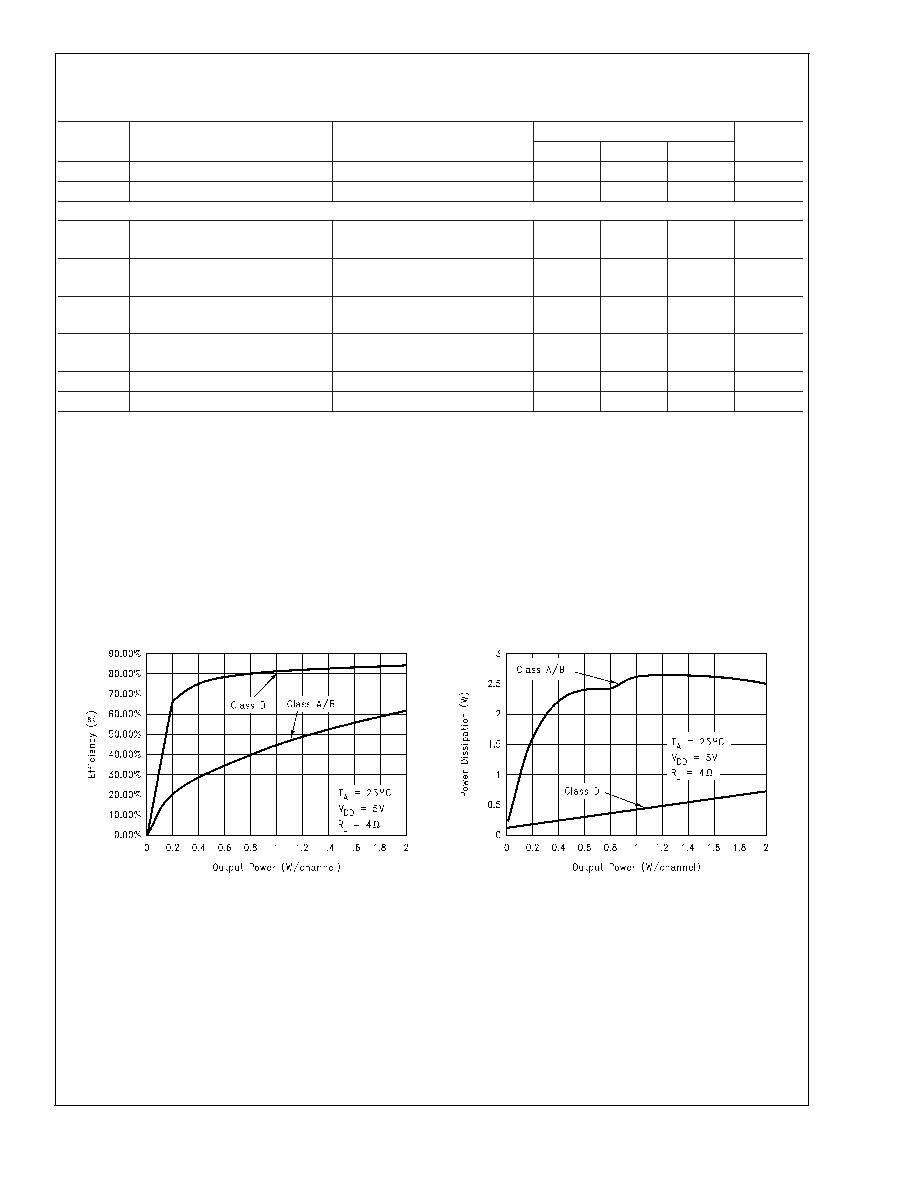
Typical Performance Characteristics
Efficiency vs Output Power
Power Dissipation vs Output Power
10126910
10126911
LM4663
www.national.com
3
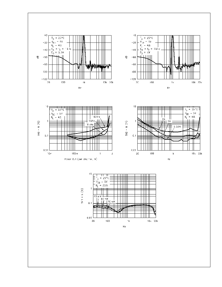
Typical Performance Characteristics
(Continued)
Class D Amplifier
In-Band Output Spectrum
Class D Amplifier
In-Band Output Spectrum
10126912
10126913
Class D Amplifier
THD + N vs Power vs Frequency
Class D Amplifier
THD + N vs Frequency vs Power
10126914
10126915
Headphone THD + N vs Frequency vs Power
10126916
LM4663
www.national.com
4
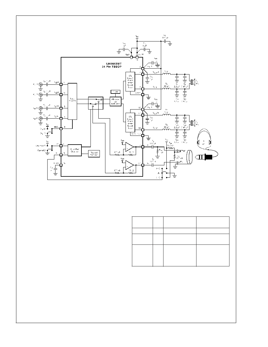
Applications Information
Suggested Application Circuit
The LM4663 achieves its specified performance using the
recommended application circuit shown in Figure 1. The
circuit provides full access to the stereo 2W/channel power
amplifiers and the 80mW/channel stereo headphone ampli-
fier. The HPSELECT (headphone select ) input is controlled
by a stereo mini-plug/jack with additional control contact.
Other applications of this device may use external generated
logic signals to control this function.
Control Pins
The LM4663 has three control pins: INSEL, SD, and HPSEL.
The INSEL pin is used to select between the two stereo
inputs, V
IN1
and V
IN2
. Connecting the INSEL pin to the
positive supply selects V
IN1
, whereas pulling it to ground
selects V
IN2
. Micropower shutdown operation is selected by
pulling the SD to the positive supply. Applying the positive
supply to the HPSEL pin selects the headphone amplifiers
and grounding the HPSEL pin selects the Class D amplifiers.
Table 1 is a summary of the function selected when applying
ground or V
DD
to the control pins.
TABLE 1. Function selected when applying V
DD
or
GND to the INSEL, SD, and HPSEL control pins.
Control
Function
Pin
Apply GND
Apply V
DD
INSEL
10
V
IN2
L & R
V
IN1
L & R
SD
9
Full power
operation
Micropower
shutdown
HPSEL
16
Deactivate
headphone amps
and activate Class
D amps
Deactivate Class
D amps and
activate
headphone amps
Output Filters
The LM4663's 2W power amplifiers use a Class D switching
topology that requires a filter between the amplifier outputs
and the load. The balanced, L-C filters shown in Figure 1 use
component values recommended for a maximally flat mag-
nitude in the pass-band and a cut-off frequency of 18kHz
with a load impedance of 4
. We do not recommend omit-
ting the filter because considerable out-of-band energy is
present in the Class D output waveform. This energy would
be dissipated in the load impedance's resistive component,
which diminishes efficiency.
10126903
FIGURE 1. Operating on a single 5V supply, this recommended application circuit is a complete solution with 2W
Class D amplifiers that drive 4
speakers and 80mW amplifiers drive 32 headphones.
LM4663
www.national.com
5