LM4668
10W High-Efficiency Mono BTL Audio Power Amplifier
General Description
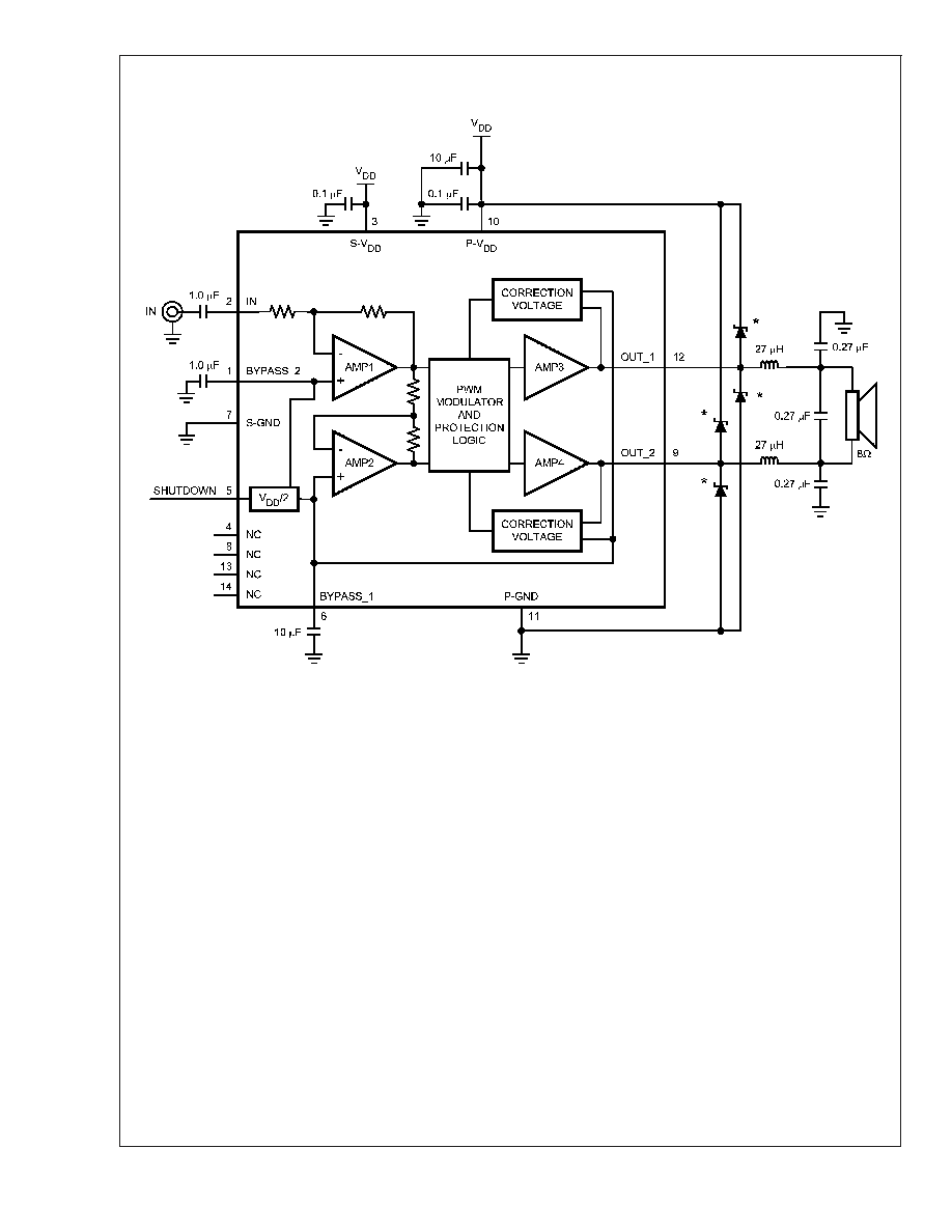
The LM4668 is a high efficiency switching audio power
amplifier primarily designed for demanding applications in
flat panel monitors and TV's. It is capable of delivering 6W to
an 8
mono BTL load with less than 1% distortion (THD+N)
from a 12V
DC
power supply.
Boomer audio power amplifiers were designed specifically to
provide high quality output power with a minimal amount of
external components. The LM4668 features a micro-power,
active-low shutdown mode, an internal thermal shutdown
protection mechanism, and short circuit protection.
The LM4668 contains advanced transient ("pop and click")
suppression circuitry that eliminates noises that would oth-
erwise occur during turn-on and turn-off transitions.
Key Specifications
j
Power Output BTL (V
DD
= 14V,
f
IN
= 1kHz, THD+N = 10%, R
L
= 8
)
10W (typ)
j
Quiescent Power Supply Current
30mA (typ)
j
Efficiency (V
DD
= 12V, f
IN
= 1kHz,
R
L
= 8
, P
OUT
= 6W)
79% (typ)
j
Shutdown Current
0.15mA (typ)
j
Fixed Gain
30dB (typ)
Features
n
Soft-start circuitry eliminates noise during turn-on
transition
n
Low current shutdown mode
n
Low quiescent current
n
6W BTL output, R
L
= 8
n
Short circuit protection
n
Fixed, internally set gain of 30dB
Applications
n
Flat Panel Monitors
n
Flat Panel TVs
n
Computer Sound Cards
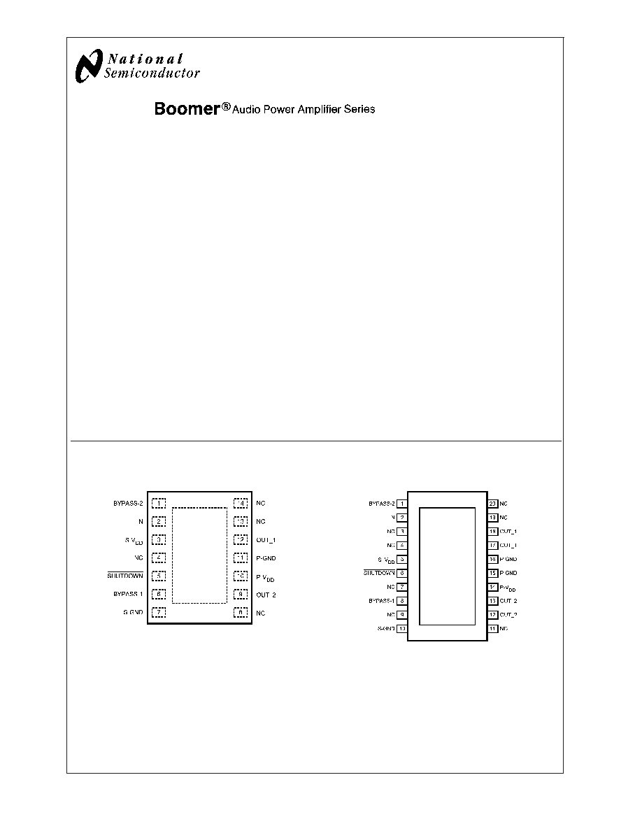
Connection Diagrams
LD Package
MH Package
20089102
Top View
Order Number LM4668LD
See NS Package Number LDC14A
200891G3
Top View
Order Number LM4668MH
See NS Package Number MXA20A
Boomer
�
is a registered trademark of National Semiconductor Corporation.
October 2004
LM4668
10W
High-Efficiency
Mono
BTL
Audio
Power
Amplifier
� 2004 National Semiconductor Corporation
DS200891
www.national.com
Absolute Maximum Ratings
(Notes 1, 2)
If Military/Aerospace specified devices are required,
please contact the National Semiconductor Sales Office/
Distributors for availability and specifications.
Supply Voltage
16V
Storage Temperature
-65�C to +150�C
Input Voltage
-0.3V to V
DD
+0.3V
Power Dissipation (Note 3)
Internally limited
ESD Susceptibility (Note 4)
2000V
ESD Susceptibility (Note 5)
200V
Junction Temperature (LD and MH)
150�C
Thermal Resistance
JC
2�C/W
JA
40�C/W
Operating Ratings
Temperature Range
T
MIN
T
A
T
MAX
-40�C
T
A
85�C
Supply Voltage (Note 10)
9V
V
DD
14.0V
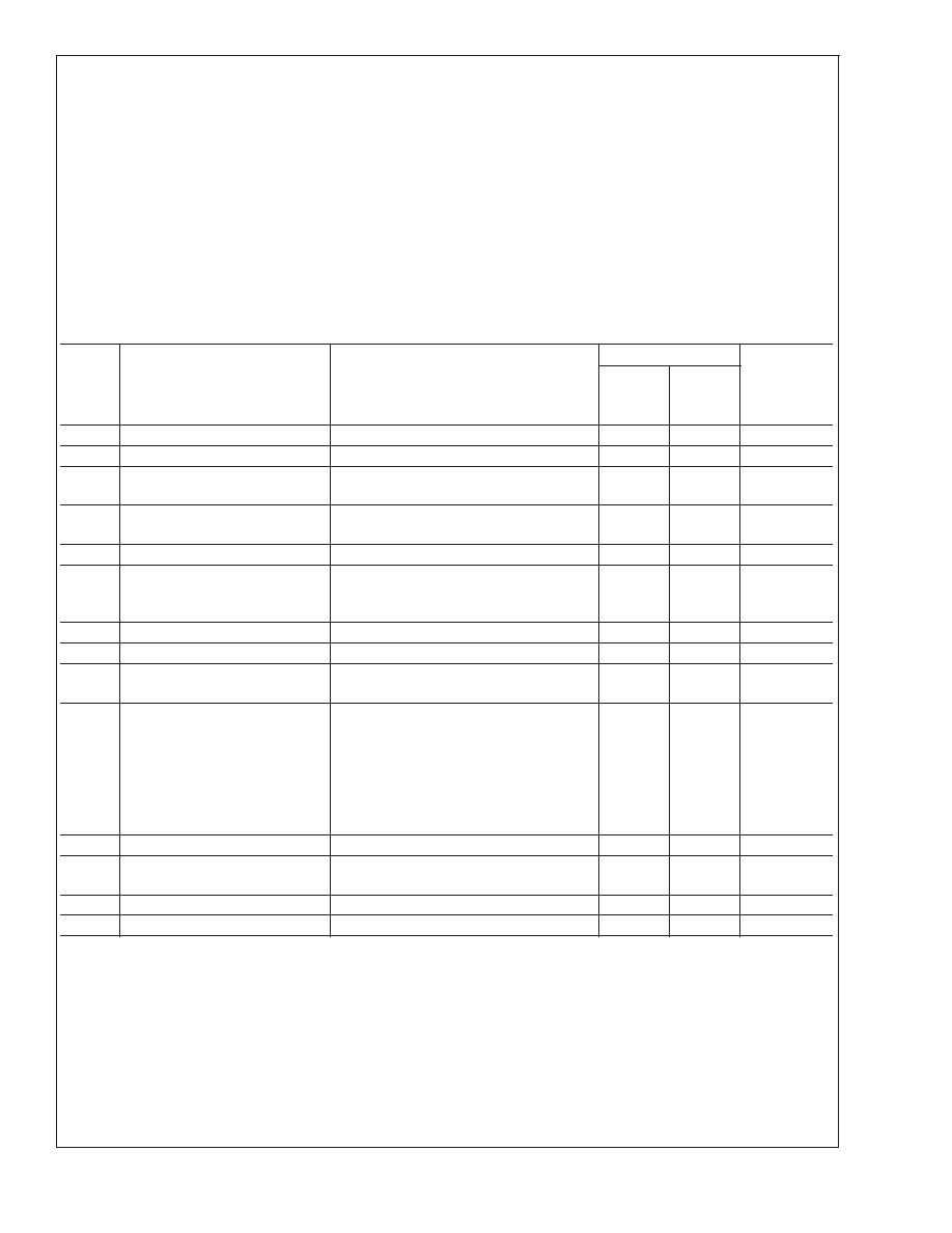
Electrical Characteristics for the LM4668
(Note 1)
The following specifications apply for the circuit shown in Figure 1 operating with V
DD
= 12V, R
L
= 8
, and f
IN
= 1kHz,
unless otherwise specified. Limits apply for T
A
= 25�C.
Symbol
Parameter
Conditions
LM4668
Units
(Limits)
Typical
Limit
(Note 6)
(Notes 7,
8)
I
DD
Quiescent Power Supply Current
V
IN
= 0V, I
O
= 0A, R
L
= 8
30
65
mA (max)
I
SD
Shutdown Current
V
SHUTDOWN
= GND (Note 9)
0.15
mA
A
V
Amplifier Gain
BTL output voltage with respect to input
voltage, V
IN
= 100mV
p-p
30
32
28
dB (max)
dB (min)
P
O
Output Power
THD+N = 1% (max)
THD+N = 10%, V
DD
= 14V
6
10
5
W (min)
W
THD+N
Total Harmonic Distortion + Noise
P
OUT
= 1W
RMS
0.2
%
f
BW
Frequency Response Bandwith
P
OUT
= 6W, post filter,
-3dB relative to the output amplitude
at 1kHz, See Figure 1
20
20000
Hz
Hz
Efficiency
P
OUT
= 6W, including output filter
79
%
�N
Output Noise
A-Weighted Filter, V
IN
= 0V
220
�V
SNR
Signal-to-Noise Ratio
A-Weighted Filter, P
OUT
= 6W
A
V
= 30dB
90
dB
PSRR
Power Supply Rejection Ratio
V
RIPPLE
= 20mV
p-p
, C
BYPASS_1
= 10�F,
input referred
f = 50Hz
f = 60Hz
f = 100Hz
f = 120Hz
f = 1kHz
79
82
85
84
75
dB
t
WU
Wake-Up time
C
BYPASS
= 10�F
600
ms
T
SD
Thermal Shutdown Temperature
170
�C (min)
�C (max)
V
SDIH
Shutdown Voltage Input High
4
V (min)
V
SDIL
Shutdown Voltage Input Low
1.5
V (max)
Note 1: All voltages are measured with respect to the GND pin unless otherwise specified.
Note 2: Absolute Maximum Ratings indicate limits beyond which damage to the device may occur. Operating Ratings indicate conditions for which the device is
functional, but do not guarantee specific performance limits. Electrical Characteristics state DC and AC electrical specifications under particular test conditions which
guarantee specific performance limits. This assumes that the device is within the Operating Ratings. Specifications are not guaranteed for parameters where no limit
is given, however, the typical value is a good indication of device performance.
Note 3: The maximum power dissipation must be de-rated at elevated temperatures and is dictated by T
JMAX
,
JA
, and the ambient temperature T
A
. The maximum
allowable power dissipation is P
DMAX
= (T
JMAX
- T
A
)/
JA
or the number given in Absolute Maximum Ratings, whichever is lower. For the LM4668 typical application
(shown in Figure 1) with V
DD
= 12V, R
L
= 8
stereo operation, the total power dissipation is 900mW.
JA
= 40�C/W
Note 4: Human body model, 100pF discharged through a 1.5k
resistor.
Note 5: Machine model, 220pF � 240pF discharged through all pins.
Note 6: Typicals are measured at 25�C and represent the parametric norm.
Note 7: Limits are guaranteed to National's AOQL (Average Outgoing Quality Level).
LM4668
www.national.com
3
Electrical Characteristics for the LM4668
(Note 1) (Continued)
Note 8: Datasheets min/max specification limits are guaranteed by design, test, or statistical analysis.
Note 9: Shutdown current is measured in a normal room environment. The SHUTDOWN pin should be driven as close as possible to GND for minimum shutdown
current.
Note 10: Please refer to "Under Voltage Protection" on page 8 under "General Features."
Typical Performance Characteristics
THD+N vs Frequency
V
DD
= 9V, R
L
= 8
, P
O
= 1W
THD+N vs Frequency
V
DD
= 12V, R
L
= 8
, P
O
= 1W
20089106
20089107
THD+N vs Frequency
V
DD
= 14V, R
L
= 8
, P
O
= 1W
THD+N vs Output Power
R
L
= 8
, V
DD
= 9V, f = 1kHz
20089108
20089109
THD+N vs Output Power
R
L
= 8
, V
DD
= 12V, f = 1kHz
THD+N vs Output Power
R
L
= 8
, V
DD
= 14V, f = 1kHz
20089110
20089111
LM4668
www.national.com
4
Typical Performance Characteristics
(Continued)
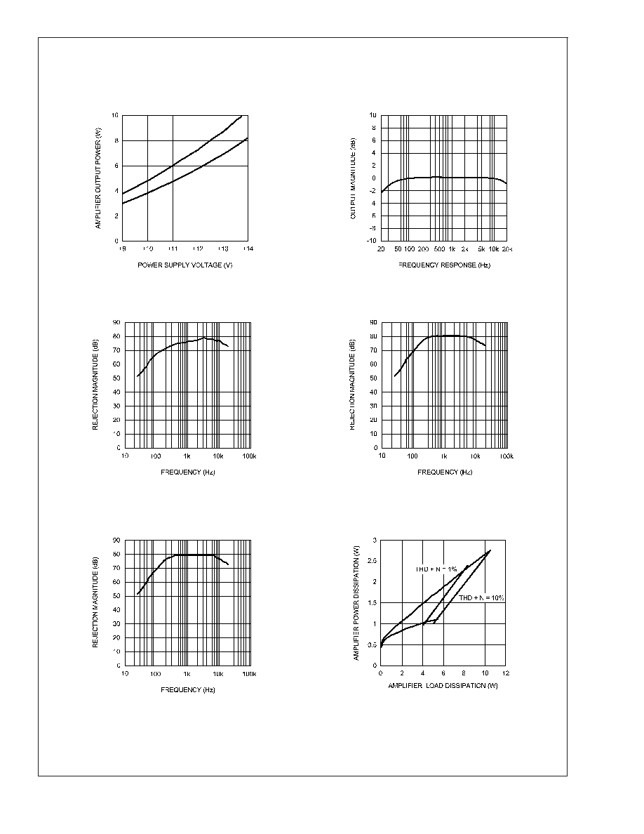
Amplifier Output Power
vs Power Supply Voltage
R
L
= 8
, f = 1kHz
Amplifier Output Magnitude
vs Frequency
R
L
= 8
, V
DD
= 12V
20089112
20089113
Power Rejection Ratio vs Frequency
V
DD
= 9V, R
L
= 8
, Input Referred
Power Rejection Ratio vs Frequency
V
DD
= 12V, R
L
= 8
, Input Referred
20089114
20089115
Power Rejection Ratio vs Frequency
V
DD
= 14V, R
L
= 8
, Input Referred
Amplifier Power Dissipation
vs Amplifier Load Dissipation
V
DD
= 14V, R
L
= 8
, f = 1kHz
20089116
20089117
LM4668
www.national.com
5