 | –≠–ª–µ–∫—Ç—Ä–æ–Ω–Ω—ã–π –∫–æ–º–ø–æ–Ω–µ–Ω—Ç: LM4670SD | –°–∫–∞—á–∞—Ç—å:  PDF PDF  ZIP ZIP |
LM4670
Filterless High Efficiency 3W Switching Audio Amplifier
General Description
The LM4670 is a fully integrated single-supply high efficiency
switching audio amplifier. It features an innovative modulator
that eliminates the LC output filter used with typical switching
amplifiers. Eliminating the output filter reduces external com-
ponent count, simplifies circuit design, and reduces board
area. The LM4670 processes analog inputs with a delta-
sigma modulation technique that lowers output noise and
THD when compared to conventional pulse width modula-
tors.
The LM4670 is designed to meet the demands of mobile
phones and other portable communication devices. Operat-
ing on a single 5V supply, it is capable of driving a 4
speaker load at a continuous average output of 2.3W with
less than 1% THD+N. Its flexible power supply requirements
allow operation from 2.4V to 5.5V.
The LM4670 has high efficiency with speaker loads com-
pared to a typical Class AB amplifier. With a 3.6V supply
driving an 8
speaker, the IC's efficiency for a 100mW
power level is 77%, reaching 88% at 600mW output power.
The LM4670 features a low-power consumption shutdown
mode. Shutdown may be enabled by driving the Shutdown
pin to a logic low (GND).
The gain of the LM4670 is externally configurable which
allows independent gain control from multiple sources by
summing the signals.
Key Specifications
j
Efficiency at 3.6V, 100mW into 8
speaker 77% (typ)
j
Efficiency at 3.6V, 600mW into 8
speaker 88% (typ)
j
Efficiency at 5V, 1W into 8
speaker
87% (typ)
j
Quiescent current, 3.6V supply
4.8mA (typ)
j
Total shutdown power supply current
0.01µA (typ)
j
Single supply range
2.4V to 5.5V
Features
n
No output filter required for inductive loads
n
Externally configurable gain
n
Very fast turn on time: 1.35ms (typ)
n
Minimum external components
n
"Click and pop" suppression circuitry
n
Micro-power shutdown mode
n
Short circuit protection
n
Available in space-saving microSMD and LLP packages
Applications
n
Mobile phones
n
PDAs
n
Portable electronic devices
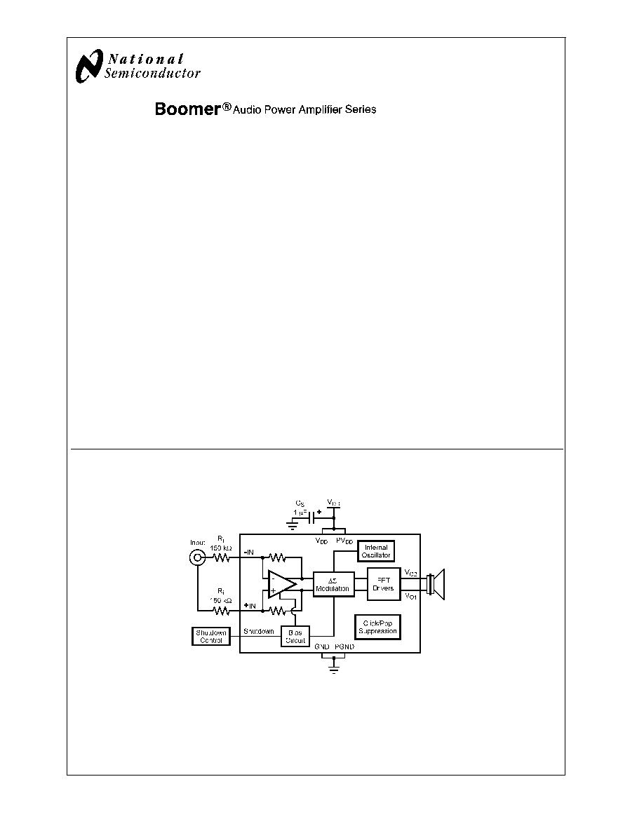
Typical Application
Boomer
Æ
is a registered trademark of National Semiconductor Corporation.
20089901
FIGURE 1. Typical Audio Amplifier Application Circuit
December 2004
LM4670
Filterless
High
Efficiency
3W
Switching
Audio
Amplifier
© 2004 National Semiconductor Corporation
DS200899
www.national.com
Connection Diagrams
9 Bump micro SMD Package
micro SMD Marking
20089936
Top View
Order Number LM4670ITL, LM4670ITLX
See NS Package Number TLA09ZZA
200899C6
Top View
X -- Date Code
T -- Die Traceability
G -- Boomer Family
E6 ≠ LM4670ITL
Leadless Leadframe Package (LLP)
LLP Marking
20089949
Top View
Order Number LM4670SD
See NS Package Number SDA08A
Contact NSC Sales Office for Availability
20089950
Top View
Z -- Plant Code
XY -- Date Code
TT -- Die Traceability
L4670 -- LM4670
LM4670
www.national.com
2
Absolute Maximum Ratings
(Notes 1, 2)
If Military/Aerospace specified devices are required,
please contact the National Semiconductor Sales Office/
Distributors for availability and specifications.
Supply Voltage (Note 1)
6.0V
Storage Temperature
-65∞C to +150∞C
Voltage at Any Input Pin
V
DD
+ 0.3V
V GND - 0.3V
Power Dissipation (Note 3)
Internally Limited
ESD Susceptibility (Note 4)
2.0kV
ESD Susceptibility (Note 5)
200V
Junction Temperature (T
JMAX
)
150∞C
Thermal Resistance
JA
(micro SMD)
220∞C/W
JA
(LLP)
64∞C/W
JC
(LLP)
TBD∞C/W
Soldering Information
See AN-1112 "microSMD Wafers Level Chip Scale
Package."
Operating Ratings
(Note 1) (Note 2)
Temperature Range
T
MIN
T
A
T
MAX
-40∞C
T
A
85∞C
Supply Voltage
2.4V
V
DD
5.5V
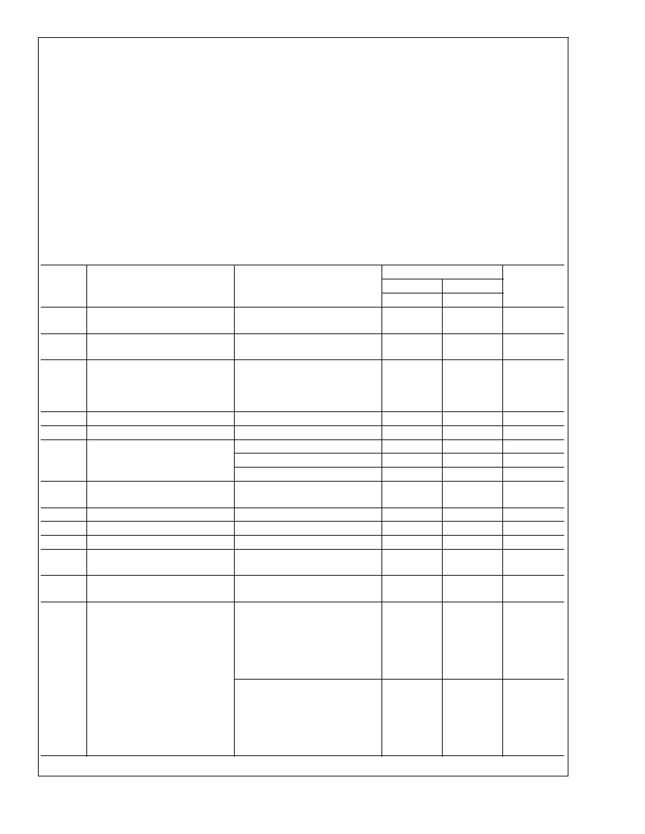
Electrical Characteristics
(Notes 1, 2)
The following specifications apply for A
V
= 2V/V (R
I
= 150k
), R
L
= 15µH + 8
+ 15µH unless otherwise specified. Limits ap-
ply for T
A
= 25∞C.
Symbol
Parameter
Conditions
LM4670
Units
(Limits)
Typical
Limit
(Note 6)
(Notes 7, 8)
|V
OS
|
Differential Output Offset Voltage
V
I
= 0V, A
V
= 2V/V,
V
DD
= 2.4V to 5.0V
25
mV (max)
PSRR
GSM
GSM Power Supply Rejection Ratio
V
DD
= 2.4V to 5.0V,
Input Referred
64
dB
CMRR
GSM
GSM Common Mode Rejection
Ratio
V
DD
= 2.4V to 5.0V
V
IC
= V
DD
/2 to 0.5V,
V
IC
= V
DD
/2 to V
DD
≠ 0.8V,
Input Referred
80
dB
|I
IH
|
Logic High Input Current
V
DD
= 5.0V, V
I
= 5.8V
20
100
µA (max)
|I
IL
|
Logic Low Input Current
V
DD
= 5.0V, V
I
= ≠0.3V
1
5
µA (max)
V
IN
= 0V, No Load, V
DD
= 5.0V
7.0
10
mA (max)
I
DD
Quiescent Power Supply Current
V
IN
= 0V, No Load, V
DD
= 3.6V
4.8
mA
V
IN
= 0V, No Load, V
DD
= 2.4V
3.8
5
mA (max)
I
SD
Shutdown Current
V
SHUTDOWN
= 0V
V
DD
= 2.4V to 5.0V
0.01
1
µA (max)
V
SDIH
Shutdown voltage input high
1.0
1.4
V (min)
V
SDIL
Shutdown voltage input low
0.8
0.4
V (max)
R
OSD
Output Impedance
V
SHUTDOWN
= 0.4V
>
100
k
A
V
Gain
300k
/R
I
270k
/R
I
330k
/R
I
V/V (min)
V/V (max)
R
SD
Resistance from Shutdown Pin to
GND
300
k
P
O
Output Power
R
L
= 15µH + 4
+ 15µH,
THD = 10% (max)
f = 1kHz, 22kHz BW
V
DD
= 5V
V
DD
= 3.6V
V
DD
= 2.5V
3.0
1.5
675
W
W
mW
R
L
= 15µH + 4
+ 15µH,
THD+N = 1% (max)
f = 1kHz, 22kHz BW
V
DD
= 5V,
V
DD
= 3.6V,
V
DD
= 2.5V,
2.3
1.2
550
W
W
mW
LM4670
www.national.com
3
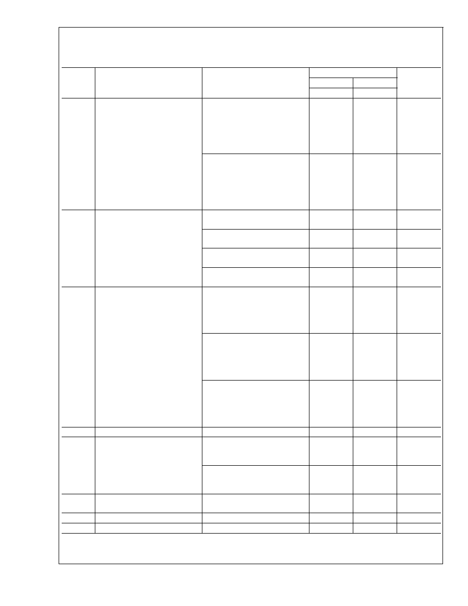
Electrical Characteristics
(Notes 1, 2)
The following specifications apply for A
V
= 2V/V (R
I
= 150k
), R
L
= 15µH + 8
+ 15µH unless otherwise specified. Limits
apply for T
A
= 25∞C. (Continued)
Symbol
Parameter
Conditions
LM4670
Units
(Limits)
Typical
Limit
(Note 6)
(Notes 7, 8)
P
O
Output Power
R
L
= 15µH + 8
+ 15µH,
THD = 10% (max)
f = 1kHz, 22kHz BW
V
DD
= 5V
V
DD
= 3.6V
V
DD
= 2.5V
1.65
850
400
W
mW
mW
R
L
= 15µH + 8
+ 15µH,
THD+N = 1% (max)
f = 1kHz, 22kHz BW
V
DD
= 5V,
V
DD
= 3.6V,
V
DD
= 2.5V,
1.35
680
325
600
W
mW (min)
mW
THD+N
Total Harmonic Distortion + Noise
V
DD
= 5V, P
O
= 1W
RMS
,
f = 1kHz
0.35
%
V
DD
= 3.6V, P
O
= 0.5W
RMS
,
f = 1kHz
0.30
%
V
DD
= 3.6V, P
O
= 0.5W
RMS
,
f = 5kHz
0.30
%
V
DD
= 3.6V, P
O
= 0.5W
RMS
,
f = 10kHz
0.30
%
V
DD
= 3.6V,
V
Ripple
= 200mV
PP
Sine,
f
Ripple
= 217Hz
Inputs to AC GND, C
I
= 0.1µ,
Input Referred
68
dB
PSRR
Power Supply Rejection Ratio
V
DD
= 3.6V,
V
Ripple
= 200mV
PP
Sine,
f
Ripple
= 1kHz
Inputs to AC GND, C
I
= 0.1µF
Input Referred
65
dB
V
DD
= 3.6V,
V
Ripple
= 200mV
PP
Sine,
f
Ripple
= 217Hz
f
IN
= 1kHz, P
O
= 10mW
RMS
Input Referred
62
dB
SNR
Signal to Noise Ratio
V
DD
= 5V, P
O
= 1W
RMS
93
dB
e
OUT
Output Noise
V
DD
= 3.6V, f = 20Hz ≠ 20kHz
Inputs to AC GND, C
I
= 0.1µF
No Weighting, Input Referred
85
µV
RMS
V
DD
= 3.6V, Inputs to AC GND
C
I
= 0.1µF, A Weighted
Input Referred
65
µV
RMS
CMRR
Common Mode Rejection Ratio
V
DD
= 3.6V, V
Ripple
= 1V
PP
Sine
f
Ripple
= 217Hz, Input Referred
80
dB
T
WU
Wake-up Time
V
DD
= 3.6V
1.35
ms
T
SD
Shutdown Time
V
DD
= 3.6V
0.01
ms
Note 1: All voltages are measured with respect to the ground pin, unless otherwise specified.
Note 2: Absolute Maximum Ratings indicate limits beyond which damage to the device may occur. Operating Ratings indicate conditions for which the device is
functional, but do not guarantee specific performance limits. Electrical Characteristics state DC and AC electrical specifications under particular test conditions which
LM4670
www.national.com
4
guarantee specific performance limits. This assumes that the device is within the Operating Ratings. Specifications are not guaranteed for parameters where no limit
is given, however, the typical value is a good indication of device performance.
Note 3: The maximum power dissipation must be derated at elevated temperatures and is dictated by T
JMAX
,
JA
, and the ambient temperature T
A
. The maximum
allowable power dissipation is P
DMAX
= (T
JMAX
≠T
A
)/
JA
or the number given in Absolute Maximum Ratings, whichever is lower. For the LM4670, T
JMAX
= 150∞C.
The typical
JA
is 220∞C/W for the microSMD package and 64∞C/W for the LLP package.
Note 4: Human body model, 100pF discharged through a 1.5k
resistor.
Note 5: Machine Model, 220pF≠240pF discharged through all pins.
Note 6: Typical specifications are specified at 25∞C and represent the parametric norm.
Note 7: Tested limits are guaranteed to National's AOQL (Average Outgoing Quality Level).
Note 8: Datasheet min/max specification limits are guaranteed by design, test, or statistical analysis.
Note 9: Shutdown current is measured in a normal room environment. Exposure to direct sunlight will increase I
SD
by a maximum of 2µA. The Shutdown pin should
be driven as close as possible to GND for minimal shutdown current and to V
DD
for the best THD performance in PLAY mode. See the Application Information
section under SHUTDOWN FUNCTION for more information.
Note 10: The performance graphs were taken using the Audio Precision AUX-0025 Switching Amplifier Measurement Filter in series with the LC filter on the board.
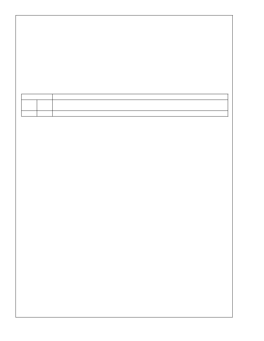
External Components Description
(Figure 1)
Components
Functional Description
1.
C
S
Supply bypass capacitor which provides power supply filtering. Refer to the Power Supply Bypassing
section for information concerning proper placement and selection of the supply bypass capacitor.
2.
R
I
Gain setting resistor. Differential gain is set by the equation A
V
= 2 * 150k
/ R
i
(V/V).
LM4670
www.national.com
5