LM4675
Ultra-Low EMI, Filterless, 2.65W, Mono, Class D Audio
Power Amplifier with Spread Spectrum
General Description
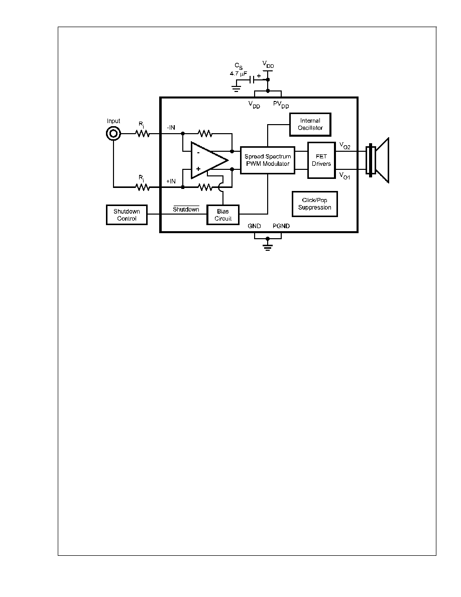
The LM4675 is a single supply, high efficiency, 2.65W, mono,
Class D audio amplifier. A spread spectrum, filterless PWM
architecture reduces EMI and eliminates the output filter,
reducing external component count, board area consump-
tion, system cost, and simplifying design.
The LM4675 is designed to meet the demands of mobile
phones and other portable communication devices. Operat-
ing on a single 5V supply, it is capable of driving a 4
speaker load at a continuous average output of 2.2W with
less than 1% THD+N. Its flexible power supply requirements
allow operation from 2.4V to 5.5V. The wide band spread
spectrum architecture of the LM4675 reduces EMI-radiated
emissions due to the modulator frequency.
The LM4675 has high efficiency with speaker loads com-
pared to a typical Class AB amplifier. With a 3.6V supply
driving an 8
speaker, the IC's efficiency for a 100mW
power level is 80%, reaching 89% at 400mW output power.
The LM4675 features a low-power consumption shutdown
mode. Shutdown may be enabled by driving the Shutdown
pin to a logic low (GND).
The gain of the LM4675 is externally configurable which
allows independent gain control from multiple sources by
summing the signals. Output short circuit and thermal over-
load protection prevent the device from damage during fault
conditions.
Key Specifications
j
Efficiency at 3.6V, 400mW into 8
speaker 89% (typ)
j
Efficiency at 3.6V, 100mW into 8
speaker 80% (typ)
j
Efficiency at 5V, 1W into 8
speaker
89% (typ)
j
Quiescent current, 3.6V supply
2.2mA (typ)
j
Total shutdown power supply current
0.01µA (typ)
j
Single supply range
2.4V to 5.5V
j
PSRR, f = 217Hz
82dB
Features
n
Spread spectrum architecture reduces EMI
n
Mono Class D Operation
n
No output filter required for inductive loads
n
Externally configurable gain
n
Very fast turn on time: 17µs (typ)
n
Minimum external components
n
"Click and pop" suppression circuitry
n
Micro-power shutdown mode
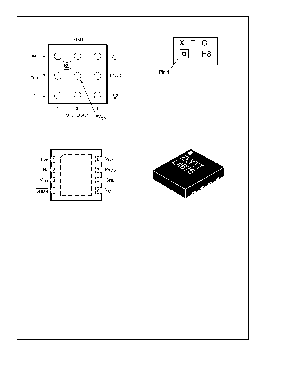
n
Available in space-saving 0.5mm pitch micro SMD and
LLP packages
Applications
n
Mobile phones
n
PDAs
n
Portable electronic devices
20182721
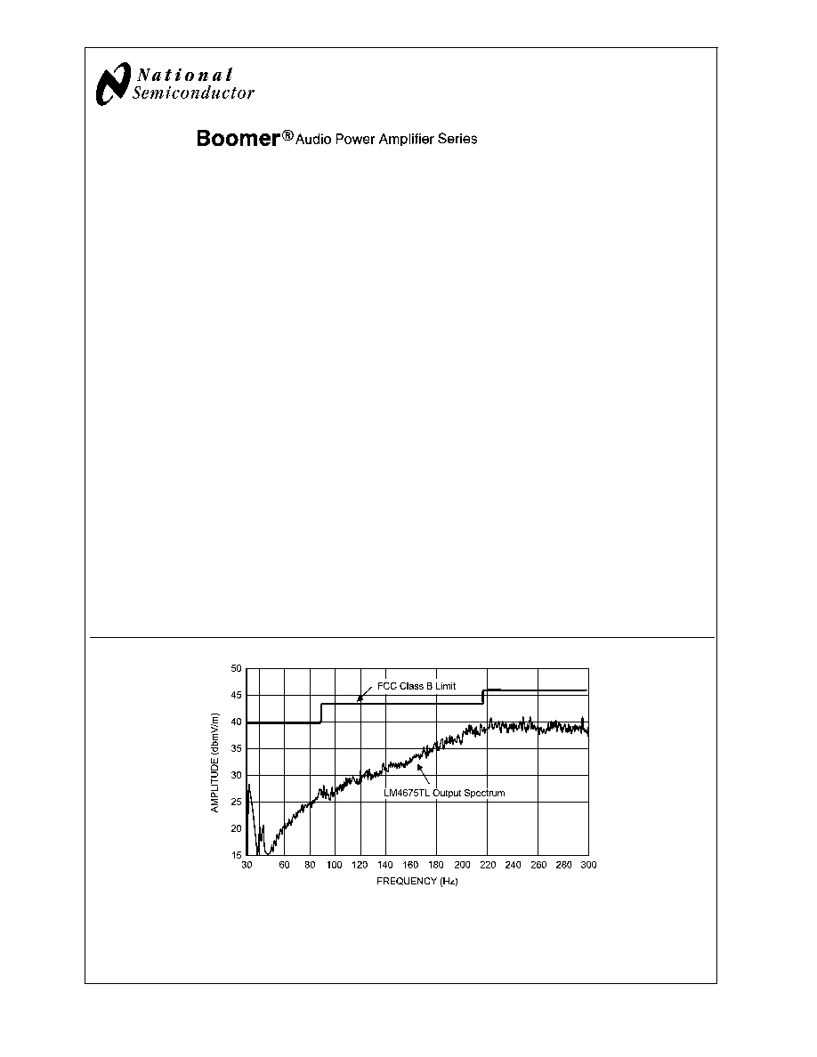
LM4675 Rf Emissions -- 6in cable
Boomer
Æ
is a registered trademark of National Semiconductor Corporation.
August 2006
LM4675
Ultra-Low
EMI,
Filterless,
2.65W
,
Mono,
Class
D
Audio
Power
Amplifier
with
Spread
Spectrum
© 2006 National Semiconductor Corporation
DS201827
www.national.com

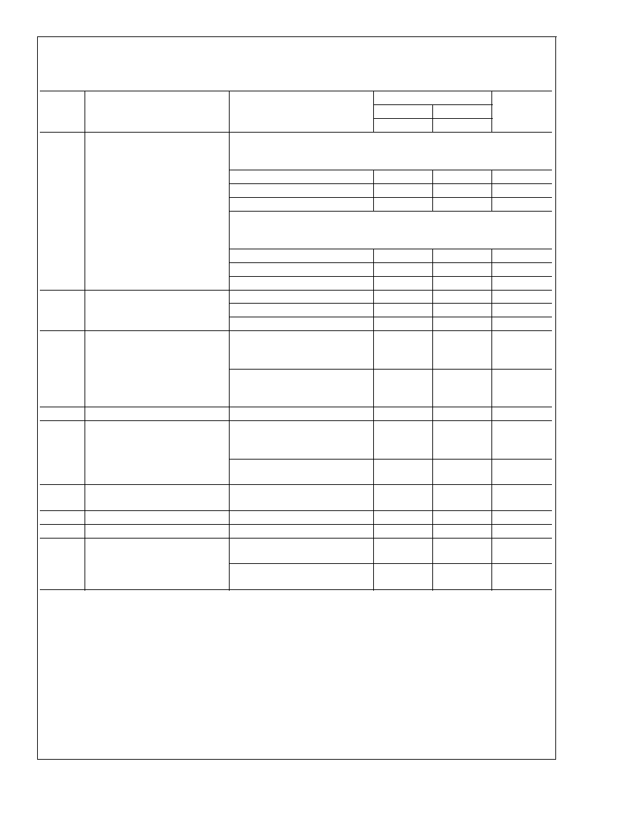
Absolute Maximum Ratings
(Notes 1, 2)
If Military/Aerospace specified devices are required,
please contact the National Semiconductor Sales Office/
Distributors for availability and specifications.
Supply Voltage (Note 1)
6.0V
Storage Temperature
-65∞C to +150∞C
Voltage at Any Input Pin
V
DD
+ 0.3V
V GND - 0.3V
Power Dissipation (Note 3)
Internally Limited
ESD Susceptibility, all other pins (Note 4)
2.0kV
ESD Susceptibility (Note 5)
200V
Junction Temperature (T
JMAX
)
150∞C
Thermal Resistance
JA
(micro SMD)
220∞C/W
JA
(LLP)
73∞C/W
Soldering Information
See AN-1112 "microSMD Wafers Level Chip Scale
Package."
Operating Ratings
(Note 1) (Note 2)
Temperature Range
T
MIN
T
A
T
MAX
-40∞C
T
A
85∞C
Supply Voltage
2.4V
V
DD
5.5V
Electrical Characteristics
(Notes 1, 2)
The following specifications apply for A
V
= 2V/V (R
I
= 150k
), R
L
= 15µH + 8
+ 15µH unless otherwise specified. Limits ap-
ply for T
A
= 25∞C.
Symbol
Parameter
Conditions
LM4675
Units
(Limits)
Typical
Limit
(Note 6)
(Notes 7, 8)
|V
OS
|
Differential Output Offset Voltage
V
I
= 0V, A
V
= 2V/V,
V
DD
= 2.4V to 5.0V
3
mV
|I
IH
|
Logic High Input Current
V
DD
= 5.0V, V
I
= 5.5V
17
100
µA (max)
|I
IL
|
Logic Low Input Current
V
DD
= 5.0V, V
I
= ≠0.3V
0.9
5
µA (max)
V
IN
= 0V, No Load, V
DD
= 5.0V
2.8
3.9
mA (max)
I
DD
Quiescent Power Supply Current
V
IN
= 0V, No Load, V
DD
= 3.6V
2.2
2.9
mA
V
IN
= 0V, No Load, V
DD
= 2.4V
1.6
2.3
mA (max)
V
IN
= 0V, R
L
= 8
, V
DD
= 5.0V
2.8
V
IN
= 0V, R
L
= 8
, V
DD
= 3.6V
2.2
V
IN
= 0V, R
L
= 8
, V
DD
= 2.4V
1.6
I
SD
Shutdown Current
V
SHUTDOWN
= 0V
V
DD
= 2.4V to 5.0V
0.01
1.0
µA (max)
V
SDIH
Shutdown voltage input high
1.4
V (min)
V
SDIL
Shutdown voltage input low
0.4
V (max)
R
OSD
Output Impedance
V
SHUTDOWN
= 0.4V
100
k
A
V
Gain
300k
/R
I
V/V (min)
V/V (max)
R
SD
Resistance from Shutdown Pin to
GND
300
k
P
O
Output Power
R
L
= 15µH + 4
+ 15µH
THD = 10% (max)
f = 1kHz, 22kHz BW
V
DD
= 5V
V
DD
= 3.6V
V
DD
= 2.5V
2.7
1.3
560
W
W
mW
R
L
= 15µH + 4
+ 15µH
THD = 1% (max)
f = 1kHz, 22kHz BW
V
DD
= 5V
V
DD
= 3.6V
V
DD
= 2.5V
2.2
1.08
450
W
W
mW
LM4675
www.national.com
4