LM4681
10 Watt Stereo CLASS D Audio Power Amplifier with
Stereo Headphone Amplifier and I
2
C/SPI Volume Control
General Description
The LM4681 is a fully integrated single supply, CLASS D
audio power amplifier solution. The LM4681 utilizes a pro-
prietary balanced pulse-width modulation technique that low-
ers output noise and THD and improves PSRR when com-
pared to conventional pulse width modulators.
The LM4681 also features a stereo headphone amplifier that
delivers 80mW into a 32
headset with less than 0.5% THD.
The LM4681's I
2
C/SPI (selectable) volume control has a
+30dB to ≠48dB range when speakers are driven and a
range of +13dB to ≠65dB when headphones are connected.
All amplifiers are protected by thermal shutdown. Addition-
ally, the high efficiency power amplifiers have output current
limit.
With a 8
load, the IC's efficiency for a 6W power level is
85%. The IC features click and pop reduction circuitry that
minimizes audible popping during device turn-on and turn-
off. The LM4681 is available in a 48-lead LLP package, ideal
for portable and desktop computer applications.
Key Specifications
n
P
O
at THD+N =10%, A
V
= 30dB, V
DD
= 14V
10W (typ)
n
THD+N at 1kHz at 1W into 8
(Power Amp) 0.43% (typ)
n
Efficiency at 7W into 8
85% (min)
n
Total quiescent power supply current
50mA (typ)
n
THD+N 1kHz, 20mW, 32
(Headphone)
0.02% (typ)
n
Single supply range
9.0V to 15.5V
Features
n
Pulse-width modulator.
n
I
2
C/SPI (selectable) volume control
n
Stereo headphone amplifier.
n
"Click and pop" suppression circuitry.
n
Micropower shutdown mode.
n
48 lead LLP package (No heatsink required).
Applications
n
Flat Panel Displays
n
Televisions
n
Multimedia Monitors
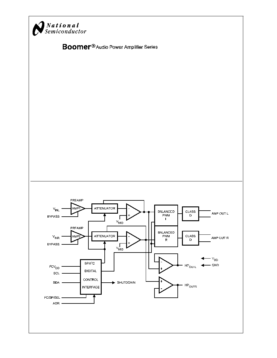
Block Diagram
20118922
Block Diagram for LM4681
BOOMER
TM
is a trademark of National Semiconductor Corporation.
March 2006
LM4681
10
W
att
Stereo
CLASS
D
Audio
Power
Amplifier
with
Stereo
Headphone
Amplifier
and
I2C/SPI
V
olume
Control
© 2006 National Semiconductor Corporation
DS201189
www.national.com
Absolute Maximum Ratings
(Note 2)
If Military/Aerospace specified devices are required,
please contact the National Semiconductor Sales Office/
Distributors for availability and specifications.
Supply Voltage
16V
Input Voltage
-0.3V to V
DD
+0.3V
Power Dissipation (Note 3)
Internally Limited
ESD Susceptibility(Note 4)
2000V
ESD Susceptibility (Note 5)
200V
Junction Temperature (Note 6)
150∞C
Storage Temperature
-65∞C
T
A
150∞C
Soldering Information
LLP Package
Vapor Phase (60 sec.)
215∞C
Infrared (15 sec.)
220∞C
Operating Ratings
(Notes 1, 2)
Temperature Range
T
MIN
T
A
T
MAX
-40∞C
T
A
+85∞C
Supply Voltage
9V
V
DD
15.5V
Thermal Resistance (LLP Package)
JA
28∞C/W
JC
20∞C/W
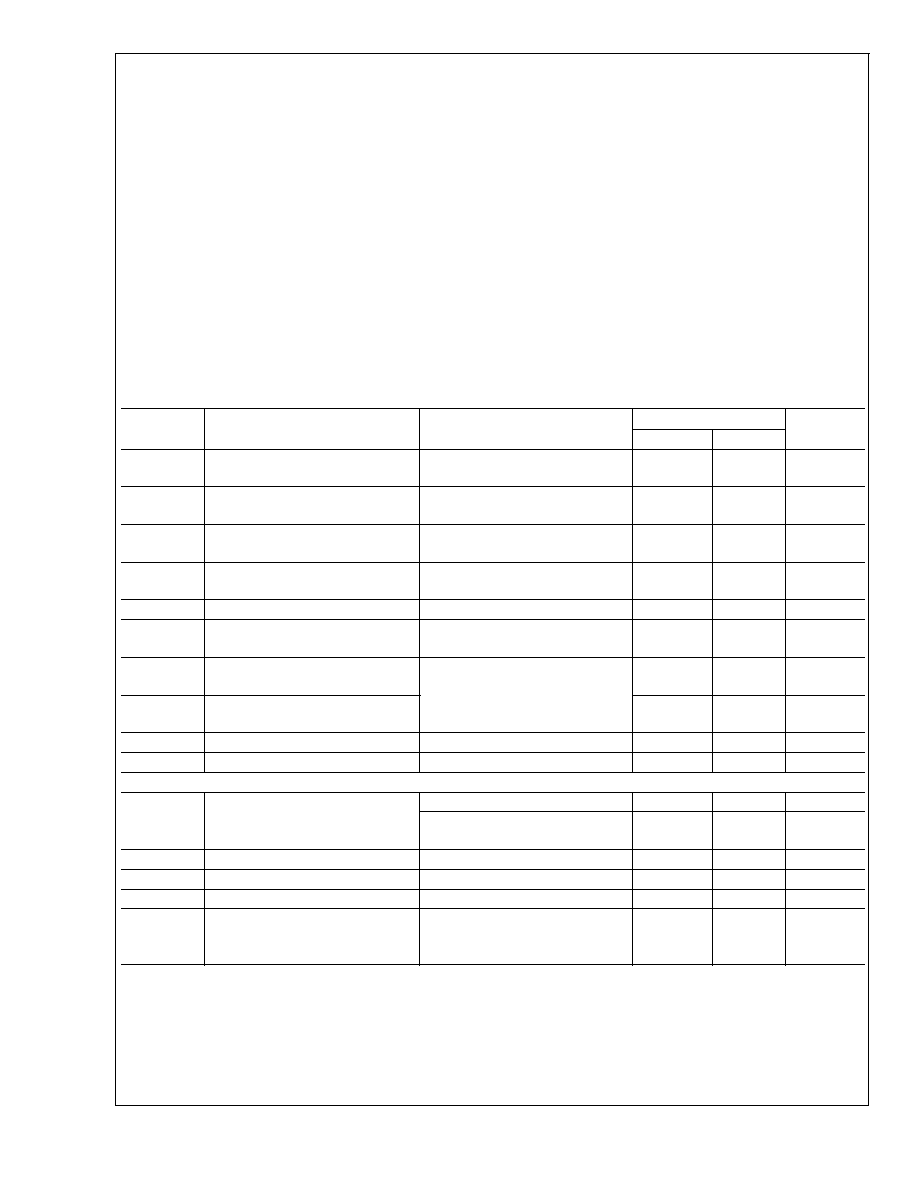
Electrical Characteristics
(Notes 1, 2, 7)
The following specifications apply for V
DD
= 12V, I
2
CV
DD
= 5V, R
L
= 8
, LC filter values as shown in Figure 1, unless other-
wise specified. Limits apply for T
A
= 25∞C.
Symbol
Parameter
Conditions
LM4681
Units
Typical
Limit
V
DD
Operating Supply Voltage Range
12
15.5
9
V (max)
V (min)
I
S
Quiescent Power Supply Current,
Class D Mode
V
IN
= 0V
RMS
, V
HPSEL
= 0V
50
70
mA
(max)
I
S
Quiescent Power Supply Current,
Headphone Mode
V
IN
= 0V
RMS
, V
HPSEL
= V
DD
22
30
mA
(max)
I
SD
Quiescent Power Supply Current,
Shutdown Mode
V
SD
= 5V
0.1
mA
R
IN
Input Resistance in Both Modes
8
k
I
2
CV
DD
I
2
C / SPI Logic Supply Voltage
5.5
3
V (max)
V (min)
V
IH
Minimum High Level Input
Voltage
I
2
C/SPI Interface pins
0.7 x
I
2
CV
DD
V (min)
V
IL
Maximum Low Level Input
Voltage
0.3 x
I
2
CV
DD
V (max)
V
HPIH
HP Sense High Input Voltage
V
DD
≠ 1
V (min)
V
HPIL
HP Sense Low Input Voltage
V
DD
/2
V (max)
Power Amplifiers
P
O
Maximum Output Power, Per
Channel
THD+N
1%, f
IN
= 1kHz
6.0
5.3
W (min)
THD+N
10%, V
DD
= 14V,
f
IN
= 1kHz
10
W
P
D1
Power Dissipation
P
O
= 6W/Chan, f
IN
= 1kHz
1.17
W
E
FF1
Efficiency
P
O
= 6W/Chan, f
IN
= 1kHz
85
%
THD+N
Harmonic Distortion + Noise
P
O
= 1W/Chan, f
IN
= 1kHz
0.11
%
V
NOISE
Output Noise Voltage
R
SOURCE
= 50
, C
IN
= 1µF,
BW = 8Hz to 22kHz,
A-weighted, input referred
10
µV
LM4681
www.national.com
4

Electrical Characteristics
(Notes 1, 2, 7) (Continued)
The following specifications apply for V
DD
= 12V, I
2
CV
DD
= 5V, R
L
= 8
, LC filter values as shown in Figure 1, unless other-
wise specified. Limits apply for T
A
= 25∞C.
Symbol
Parameter
Conditions
LM4681
Units
Typical
Limit
PSRR
Power Supply Rejection Ratio
V
RIPPLE
= 200mV
P-P
,
C
BYPASS1
= 10µF,
input referred
f = 50Hz
f = 60Hz
f = 100Hz
f = 120Hz
f = 1kHz
82
84
92
95
95
dB
Headphone Amplifiers
P
O
Maximum Power Output Per
Channel
THD+N
1%, R
L
= 32
,
f
IN
= 1kHz
94
70
mW
(min)
THD+N
Distortion + Noise
P
O
= 20mW, R
L
= 32
,
f
IN
= 1kHz
0.02
%
V
NOISE
Output Noise Voltage, RMS
R
IN
= 50
, C
IN
= 1µF,
BW = 20Hz to 20kHz, R
L
= 32
A-weighted, Input referred
22
µV
PSRR
Power Supply Rejection Ratio
(Referred to Input)
200mV, 1kHz, V
IN
= 0, R
L
= 32
77
dB
Electrical Characteristics for Volume Control
(Notes 1, 2)
The following specifications apply for V
DD
= 12V. Limits apply for T
A
= 25∞C.
Symbol
Parameter
Conditions
LM4681
Units
(Limits )
Typical
(Note 8)
Limit
(Note 7)
C
RANGE
Gain Range
Digital Code = Full Scale, No Load
Power Amplifier
Headphone Amplifier
30
13
29
12
dB (min)
dB (min)
Digital Code = +1LSB, No Load
Power Amplifier
Headphone Amplifier
≠48
≠65
≠46
≠63
dB (min)
dB (min)
A
M
Mute Gain
Digital Code = 0, No Load
Power Amplifier
Headphone Amplifier
≠76
≠74
≠74
dB (max)
dB (max)
Note 1: All voltages are measured with respect to the ground pin, unless otherwise specified.
Note 2: "Absolute Maximum Ratings" indicate limits beyond which damage to the device may occur. "Operating Ratings" indicate conditions for which the device
is functional, but do not guarantee specific performance limits. "Electrical Characteristics" state DC and AC electrical specifications under particular test conditions
which guarantee specific performance limits. This assumes that the device is within the Operating Ratings. Specifications are not guaranteed for parameters where
no limit is given, however, the typical value is a good indication of device performance.
Note 3: For operating at case temperatures above 25∞C, the device must be derated based on a 150∞C maximum junction temperature and a thermal resistance
of
JA
= 80∞C/W (junction to ambient).
Note 4: Human body model, 100pF discharged through a 1.5k
resistor.
Note 5: Machine Model 220pF - 240pF discharged through all pins.
Note 6: The operating junction temperature maximum is 150∞C.
Note 7: Limits are guaranteed to National's AOQL (Average Outgoing Quality Level).
Note 8: Typicals are measured at 25∞C and represent the parametric norm.
LM4681
www.national.com
5