 | –≠–ª–µ–∫—Ç—Ä–æ–Ω–Ω—ã–π –∫–æ–º–ø–æ–Ω–µ–Ω—Ç: LM4702CTA | –°–∫–∞—á–∞—Ç—å:  PDF PDF  ZIP ZIP |
LM4702 Overture
Æ
Audio Power Amplifier Series
Stereo High Fidelity 200 Volt* Driver with Mute
General Description
The LM4702 is a high fidelity audio power amplifier driver
designed for demanding consumer and pro-audio applica-
tions. Amplifier output power may be scaled by changing the
supply voltage and number of output devices. The LM4702
is capable of delivering in excess of 300 watts per channel
single ended into an 8 ohm load in the presence of 10% high
line headroom and 20% supply regulation.
The LM4702 includes thermal shut down circuitry that acti-
vates when the die temperature exceeds 150∞C. The
LM4702's mute function, when activated, mutes the input
drive signal and forces the amplifier output to a quiescent
state.
The LM4702 is available in 3 grades that span a wide range
of applications and performance levels. The LM4702C is
targeted at high volume applications. The LM4702B (in de-
velopment) includes a higher voltage rating along with the
tighter specifications. The LM4702A (in development) is the
premium part with the highest voltage rating, fully specified
with limits over voltage and temperature, and is offered in a
military 883 compliant TO-3 package.
* Tentative Max Operating voltage for the LM4702A,
LM4702B (in development)
Key Specifications
j
Wide operating voltage range
LM4702A (in development)
±
20V to
±
85V
LM4702B (in development)
±
20V to
±
80V
LM4702C
±
20V to
±
75V
j
Equivalent Noise
3µV
j
PSRR
110dB (typ)
j
THD
0.001%
Features
n
Very high voltage operation
n
Scalable output power
n
Minimum external components
n
External compensation
n
Thermal Shutdown and Mute
Applications
n
AV receivers
n
Audiophile power amps
n
Pro Audio
n
High voltage industrial applications
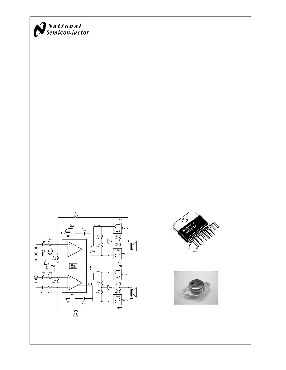
Typical Application and Connection Diagrams
20158319
FIGURE 1. Typical Audio Amplifier Application Circuit
20158302
Plastic Package -- 15 Lead TO-220
(for LM4702; LM4702B, in development)
20158320
Metal Can -- 15 Lead TO-3
(for LM4702A, in development)
Overture
Æ
is a registered trademark of National Semiconductor Corporation.
November 2005
LM4702
Overture
Æ
Stereo
High
Fidelity
200
V
olt*
Driver
with
Mute
© 2005 National Semiconductor Corporation
DS201583
www.national.com
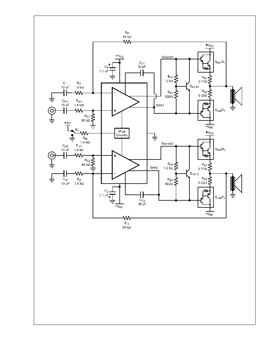
Typical Application and Connection Diagrams
(Continued)
20158319
FIGURE 1. Typical Audio Amplifier Application Circuit
LM4702
www.national.com
2
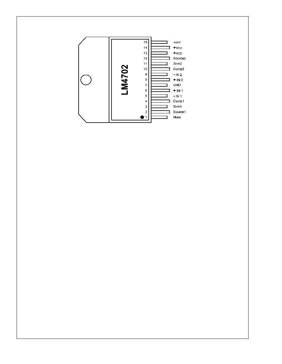
Connection Diagram
Plastic Package (For B and C) (Note 13)
20158301
Top View
Order Number LM4702T(B & C)
See NS Package Number TA15A
LM4702
www.national.com
3
Absolute Maximum Ratings
(Notes 1,
2)
If Military/Aerospace specified devices are required,
please contact the National Semiconductor Sales Office/
Distributors for availability and specifications.
Supply Voltage |V
+
| + |V
-
|
200V
Differential Input Voltage
+/-6V
Common Mode Input Range
0.4 Vee to 0.4 Vcc
Power Dissipation (Note 3)
4W
ESD Susceptibility (Note 4)
1.5kV
ESD Susceptibility (Note 5)
200V
Junction Temperature (T
JMAX
) (Note 9)
150∞C
Soldering Information
T Package (10 seconds)
260∞C
Storage Temperature
-40∞C to +150∞C
Thermal Resistance
JA
30∞C/W
JC
1∞C/W
Operating Ratings
(Notes 1, 2)
Temperature Range
T
MIN
T
A
T
MAX
-20∞C
T
A
+75∞C
Supply Voltage |V
+
| + |V
-
|
LM4702A (in development)
+/-20V
V
TOTAL
+/-85V
LM4702B (in development)
+/-20V
V
TOTAL
+/-80V
LM4702C
+/-20V
V
TOTAL
+/-75V
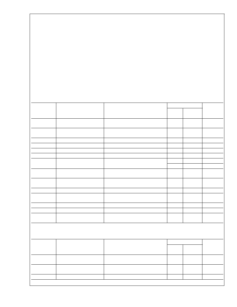
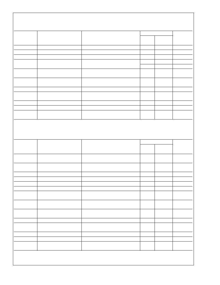
Electrical Characteristics (LM4702C) Vcc = +75V, Vee = ≠75V
(Notes 1, 2)
The following specifications apply for I
MUTE
= 1.5mA, unless otherwise specified. Limits apply for T
A
= 25∞C.
Symbol
Parameter
Conditions
LM4702
Units
(Limits)
Typical
Limit
(Note 6)
(Notes 7, 8)
I
CC
Total Quiescent Power Supply
Current
V
CM
= 0V, V
O
= 0V, I
O
= 0A
25
30
mA (max)
THD+N
Total Harmonic Distortion +
Noise
No load, A
V
= 30dB
V
OUT
= 14V
RMS
@
1kHz
0.005
%
R
S
Input Bias Resistor
50
100
k
(max)
Av
Closed Loop Voltage Gain
26
dB (min)
Av open
Open Loop Gain
Vin = 1mVrms, f = 1KHz, C = 30pF
93
dB
Vom
Output Voltage Swing
THD = 0.05%, Freq = 20Hz to 20KHz
51
Vrms (min)
Vnoise
Output Noise
Rs = 10k
, LPF = 30kHz, Av = 30dB
A-weighted
150
300
µV (max)
90
µV
I
OUT
Output Current
Current from Source to Sink Pins
5.5
3
10
mA(min)
mA (max)
I
mute
Current into Mute Pin
To put part in "play" mode
1.5
1
2
mA(min)
mA (max)
X
TALK
Channel Separation (Note 11)
f = 1kHz
@
Av = 30dB
85
dB
SR
Slew Rate
V
IN
= 1.2V
P-P
, f = 10kHz square Wave,
Outputs shorted
15
V/µs
V
OS
Input Offset Voltage
V
CM
= 0V, I
O
= 0mA
10
35
mV (max)
I
B
Input Bias Current
V
CM
= 0V, I
O
= 0mA
500
nA
PSRR
Power Supply Rejection Ratio
Rs = 1k, f = 100Hz,
Vripple = 1Vrms, Input Referred
110
95
dB (min)
Electrical Characteristics (LM4702C) Vcc = +50V, Vee = ≠50V
(Notes 1, 2)
The following specifications apply for I
MUTE
= 1.5mA, unless otherwise specified. Limits apply for T
A
= 25∞C.
Symbol
Parameter
Conditions
LM4702
Units
(Limits)
Typical
Limit
(Note 6)
(Notes 7, 8)
I
CC
Total Quiescent Power Supply
Current
V
CM
= 0V, V
O
= 0V, I
O
= 0A
22
30
mA (max)
THD+N
Total Harmonic Distortion +
Noise
No load, A
V
= 30dB
V
OUT
= 10V
RMS
@
1kHz
0.005
%
R
S
Input Bias Resistor
50
100
k
(max)
LM4702
www.national.com
4
Electrical Characteristics (LM4702C) Vcc = +50V, Vee = ≠50V
(Notes 1,
2) (Continued)
The following specifications apply for I
MUTE
= 1.5mA, unless otherwise specified. Limits apply for T
A
= 25∞C.
Symbol
Parameter
Conditions
LM4702
Units
(Limits)
Typical
Limit
(Note 6)
(Notes 7, 8)
Av
Closed Loop Voltage Gain
26
dB (min)
Av open
Open Loop Gain
Vin = 1mVrms, f = 1KHz, C = 30pF
93
dB
Vom
Output Voltage Swing
THD = 0.05%, Freq = 20Hz to 20KHz
33
Vrms (min)
Vnoise
Output Noise
Rs = 10k
, LPF = 30kHz, Av = 30dB
A-weighted
150
300
µV (max)
90
µV
I
OUT
Output Current
Outputs Shorted
5.2
3
10
mA(min)
mA (max)
I
mute
Current into Mute Pin
To put part in "play" mode
1.5
1
2
mA(min)
mA (max)
X
TALK
Channel Separation (Note 11)
f = 1kHz at Av = 30dB
85
dB
SR
Slew Rate
V
IN
= 1.2V
P-P
, f = 10kHz square Wave,
Outputs shorted
15
V/µs
V
OS
Input Offset Voltage
V
CM
= 0V, I
O
= 0mA
10
35
mV (max)
I
B
Input Bias Current
V
CM
= 0V, I
O
= 0mA
500
nA
PSRR
Power Supply Rejection Ratio
Rs = 1k, f = 100Hz,
Vripple = 1Vrms, Input Referred
110
95
dB (min)
Electrical Characteristics (LM4702B) Vcc = +80V, Vee = ≠80V (Pre-release
information)
(Notes 1, 2)
The following specifications apply for I
MUTE
= 1.5mA, unless otherwise specified. Limits apply for T
A
= 25∞C.
Symbol
Parameter
Conditions
LM4702
Units
(Limits)
Typical
Limit
(Note 6)
(Notes 7, 8)
I
CC
Total Quiescent Power Supply
Current
V
CM
= 0V, V
O
= 0V, I
O
= 0A
27
TBD
mA (max)
THD+N
Total Harmonic Distortion +
Noise
No load, A
V
= 30dB
V
OUT
= 20V
RMS
@
1kHz
0.003
TBD
% (max)
R
S
Input Bias Resistor
50
TBD
k
(max)
Av
Closed Loop Voltage Gain
TBD
dB (min)
Av open
Open Loop Gain
Vin = 1mVrms, f = 1KHz, C = 30pF
93
dB
Vom
Output Voltage Swing
THD = 0.05%, Freq = 20Hz to 20KHz
54
TBD
Vrms (min)
Vnoise
Output Noise
Rs = 10k
, LPF = 30kHz, Av = 30dB
A-weighted
150
90
TBD
TBD
µV (max)
I
OUT
Output Current
Outputs Shorted
5.5
TBD
TBD
mA(min)
mA (max)
I
mute
Current into Mute Pin
To put part in "play" mode
1.5
TBD
TBD
mA(min)
mA (max)
X
TALK
Channel Separation (Note 11)
f = 1kHz at Av = 30dB
85
TBD
dB (min)
SR
Slew Rate
V
IN
= 1.2V
P-P
, f = 10kHz square Wave,
Outputs shorted
17
TBD
V/µs (min)
V
OS
Input Offset Voltage
V
CM
= 0V, I
O
= 0mA
7
TBD
mV (max)
I
B
Input Bias Current
V
CM
= 0V, I
O
= 0mA
350
TBD
nA (max)
PSRR
Power Supply Rejection Ratio
Rs = 1k, f = 100Hz,
Vripple = 1Vrms, Input Referred
110
TBD
dB (min)
LM4702
www.national.com
5