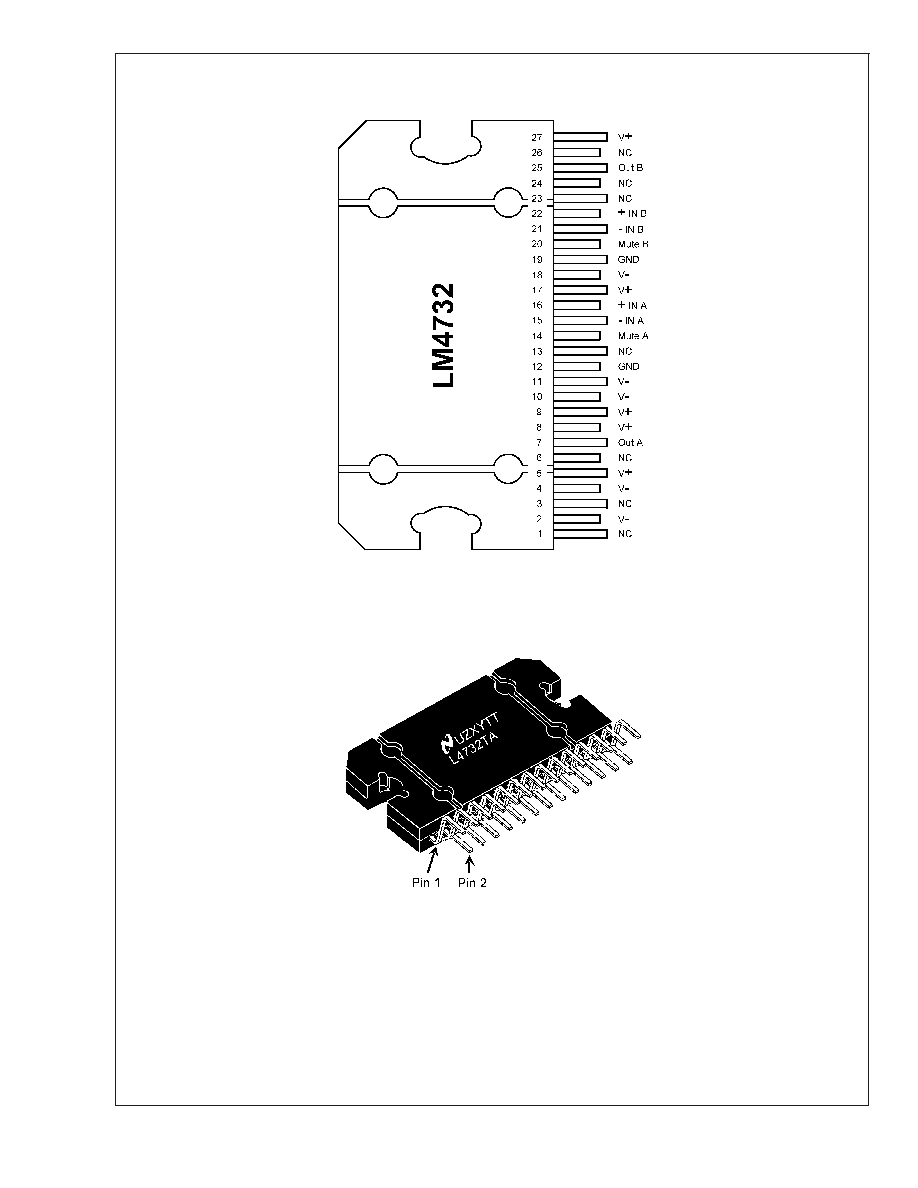
LM4732
Stereo 50W Audio Power Amplifier with Mute
General Description
The LM4732 is a stereo audio amplifier capable of typically
delivering 50W per channel of continuous average output
power into a 4
or 8 load with less than 10% THD+N from
20Hz - 20kHz.
The LM4732 has short circuit protection and a thermal shut
down feature that is activated when the die temperature
exceeds 150°C. The LM4732 also has an under voltage lock
out feature for click and pop free power on and off.
Each amplifier of the LM4732 has an independent smooth
transition fade-in/out mute.
The LM4732 has a wide operating supply range from +/-10V
- +/-40V allowing for lower cost unregulated power supplies
to be used.
The LM4732 amplifiers can easily be configured for bridge or
parallel operation for 100W mono solutions.
Key Specifications
j
Output Power/Channel at 10% THD+N,
1kHz into 4
or 8
50W (typ)
j
THD+N at 2 x 1W into 8
, 1kHz
0.01% (typ)
j
Mute Attenuation
110dB (typ)
j
PSRR
89dB (typ)
j
Slew Rate
19V/µs (typ)
Features
n
Low external component count
n
Quiet fade-in/out mute mode
n
Wide supply range: 20V - 80V
Applications
n
Audio amplifier for component stereo
n
Audio amplifier for compact stereo
n
Audio amplifier for self-powered speakers
n
Audio amplifier for high-end and HD TVs
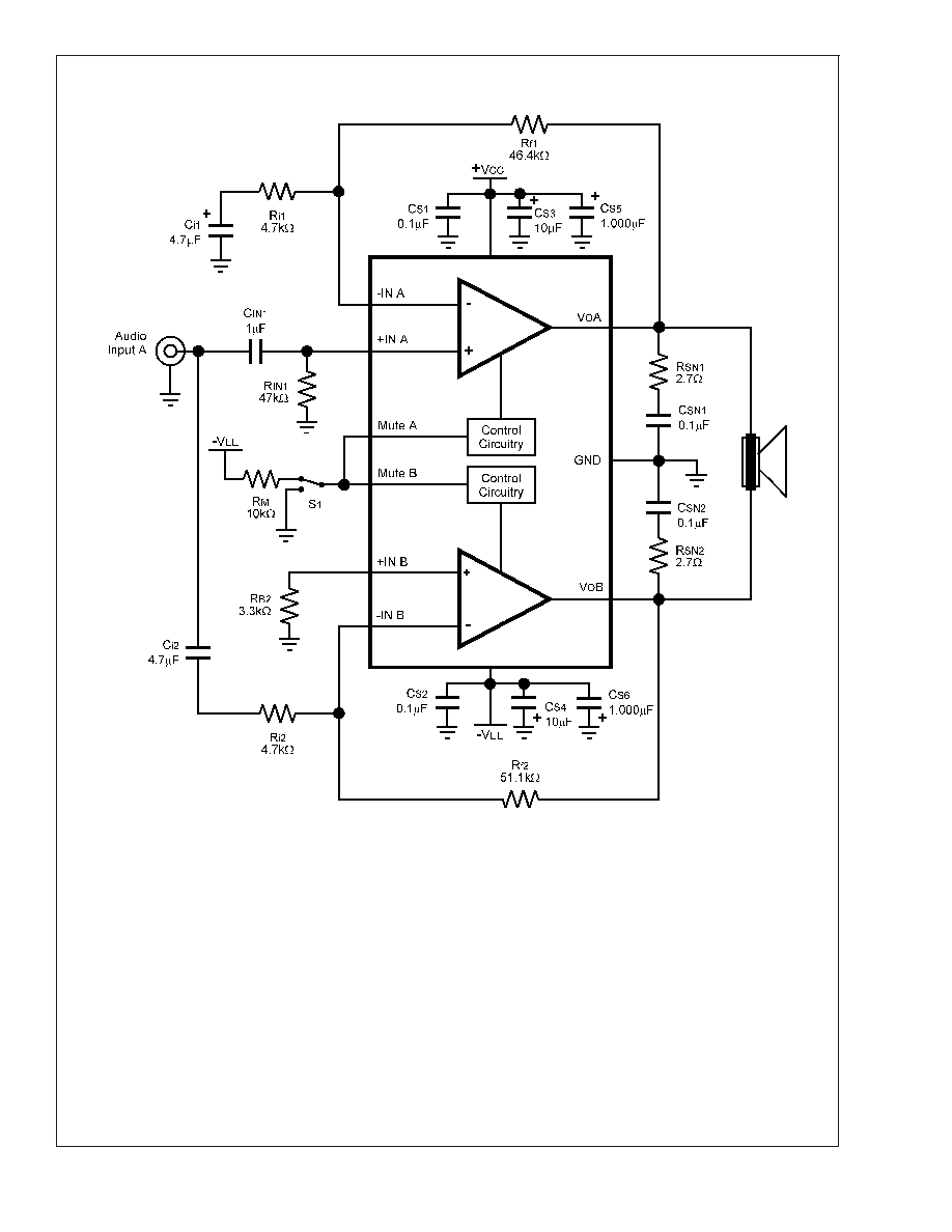
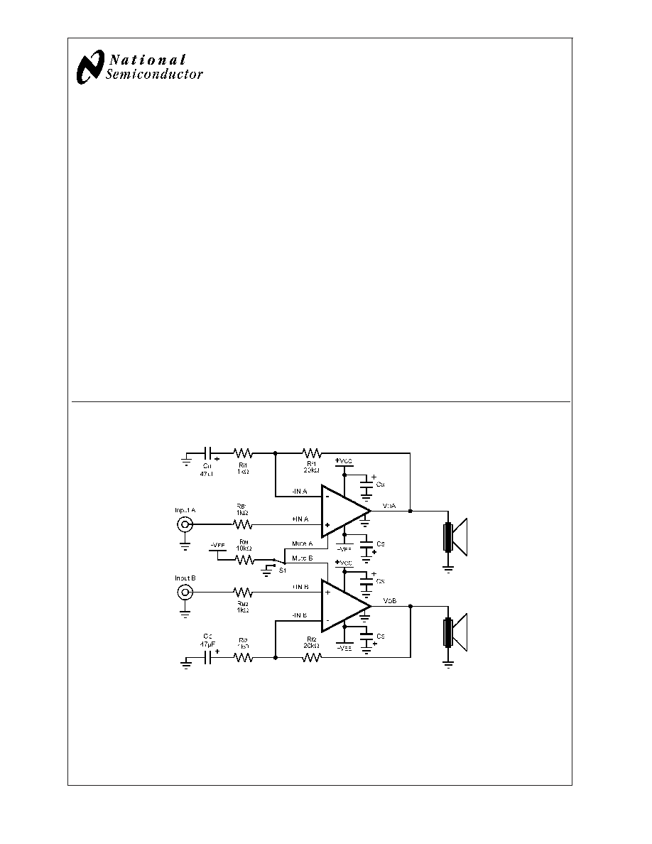
Typical Application
20072422
FIGURE 1. Typical Audio Amplifier Application Circuit
July 2003
LM4732
Stereo
50W
Audio
Power
Amplifier
with
Mute
© 2003 National Semiconductor Corporation
DS200724
www.national.com
Absolute Maximum Ratings
(Notes 1,
2)
If Military/Aerospace specified devices are required,
please contact the National Semiconductor Sales Office/
Distributors for availability and specifications.
Supply Voltage |V
+
| + |V
-
|
80V
Common Mode Input Voltage
(V
+
or V
-
) and
|V
+
| + |V
-
|
80V
Differential Input Voltage (Note 12)
60V
Output Current
Internally Limited
Power Dissipation (Note 3)
125W
ESD Susceptability (Note 4)
3.0kV
ESD Susceptability (Note 5)
200V
Junction Temperature (T
JMAX
) (Note 9)
150°C
Soldering Information
TA Package (10 seconds)
260°C
Storage Temperature
-40°C to +150°C
Thermal Resistance
JA
30°C/W
JC
0.8°C/W
Operating Ratings
(Notes 1, 2)
Temperature Range
T
MIN
T
A
T
MAX
-20°C
T
A
+85°C
Supply Voltage |V
+
| + |V
-
|
20V
V
TOTAL
80V
Electrical Characteristics
(Notes 1, 2)
The following specifications apply for V
+
= +29V, V
-
= -29V, I
MUTE
= -1mA/Channel and R
L
= 8
unless otherwise specified.
Limits apply for T
A
= 25°C.
Symbol
Parameter
Conditions
LM4732
Units
(Limits)
Typical
Limit
(Note 6)
(Notes 7, 8)
|V
+
| + |V
-
|
Power Supply Voltage (Note
10)
V
PIN7
- V
-
9V
18
20
80
V (min)
V (max)
A
M
Mute Attenuation
I
MUTE
= 0mA
110
dB
P
O
Output Power (RMS)
THD+N =10% (max), f = 1kHz
|V
+
| = |V
-
| = 22V, R
L
= 4
|V
+
| = |V
-
| = 29V, R
L
= 8
50
50
45
45
W (min)
W (min)
THD+N =1% (max), f = 1kHz
|V
+
| = |V
-
| = 22V, R
L
= 4
|V
+
| = |V
-
| = 29V, R
L
= 8
42
42
W
W
THD+N
Total Harmonic Distortion +
Noise
P
O
= 1W, f = 1kHz
A
V
= 26dB
|V
+
| = |V
-
| = 22V, R
L
= 4
|V
+
| = |V
-
| = 29V, R
L
= 8
0.02
0.01
%
%
X
talk
Channel Separation (Note 11)
P
O
= 10W, f = 1kHz
70
dB
P
O
= 10W, f = 10kHz
72
dB
SR
Slew Rate
V
IN
= 2.0V
P-P
, t
RISE
= 2ns
19
V/µs
I
DD
Total Quiescent Power
V
CM
= 0V,
105
170
mA (max)
Supply Current
V
O
= 0V, I
O
= 0A
V
OS
Input Offset Voltage
V
CM
= 0V, I
O
= 0mA
1
10
mV (max)
I
B
Input Bias Current
V
CM
= 0V, I
O
= 0mA
0.2
µA
PSRR
Power Supply Rejection Ratio
V
EE
= -29V + V
RIPPLE
= 1V
RMS
f
RIPPLE
= 120Hz sine wave, V
CC
= 29V
DC
62
dB
V
CC
= 29V + V
RIPPLE
= 1V
RMS
f
RIPPLE
= 120Hz sine wave, V
EE
=
-29V
DC
89
dB
A
VOL
Open Loop Voltage Gain
R
L
= 2k
, V
O
= 40V
115
dB
e
IN
Input Noise
IHF-A-Weighting Filter,
R
IN
= 600
(Input Referred)
2.0
µV
Note 1: All voltages are measured with respect to the ground pins, unless otherwise specified.
Note 2: Absolute Maximum Ratings indicate limits beyond which damage to the device may occur. Operating Ratings indicate conditions for which the device is
functional, but do not guarantee specific performance limits. Electrical Characteristics state DC and AC electrical specifications under particular test conditions which
guarantee specific performance limits. This assumes that the device is within the Operating Ratings. Specifications are not guaranteed for parameters where no limit
is given; however, the typical value is a good indication of device performance.
LM4732
www.national.com
3

Electrical Characteristics
(Notes 1, 2) (Continued)
Note 3: The maximum power dissipation must be de-rated at elevated temperatures and is dictated by T
JMAX
,
JC
, and the ambient temperature T
A
. The maximum
allowable power dissipation is P
DMAX
= (T
JMAX
-T
A
)/
JC
or the number given in the Absolute Maximum Ratings, whichever is lower. For the LM4732, T
JMAX
= 150°C
and the typical
JC
is 0.8°C/W. Refer to the Thermal Considerations section for more information.
Note 4: Human body model, 100pF discharged through a 1.5k
resistor.
Note 5: Machine Model: a 220pF - 240pF discharged through all pins.
Note 6: Typical specifications are measured at 25°C and represent the parametric norm.
Note 7: Tested limits are guaranteed to National's AOQL (Average Outgoing Quality Level).
Note 8: Datasheet min/max specification limits are guaranteed by design, test, or statistical analysis.
Note 9: The maximum operating junction temperature is 150°C. However, the instantaneous Safe Operating Area temperature is 250°C.
Note 10: V
-
must have at least - 9V at its pin with reference to GND in order for the under-voltage protection circuitry to be disabled. In addition, the voltage
differential between V
+
and V
-
must be greater than 14V.
Note 11: Cross talk performance was measured using the demo board shown in the datasheet. PCB layout will affect cross talk. It is recommended that input and
output traces be separated by as much distance as possible. Return ground traces from outputs should be independent back to a single ground point and use as
wide of traces as possible.
Note 12: The Differential Input Voltage Absolute Maximum Rating is based on supply voltages V
+
= 40V and V
-
= - 40V.
Note 13: The TA27A is a non-isolated package. The package's metal back, and any heat sink to which it is mounted are connected to the V
-
potential when using
only thermal compound. If a mica washer is used in addition to thermal compound,
CS
(case to sink) is increased, but the heat sink will be electrically isolated from
V
-
.
Note 14: CCIR/ARM: A Practical Noise Measurement Method; by Ray Dolby, David Robinson and Kenneth Gundry, AES Preprint No. 1353 (F-3).
LM4732
www.national.com
4