LM4752
Stereo 11W Audio Power Amplifier
General Description
The LM4752 is a stereo audio amplifier capable of delivering
11W per channel of continuous average output power to a
4
load, or 7W per channel into 8
using a single 24V sup-
ply at 10% THD+N.
The LM4752 is specifically designed for single supply opera-
tion and a low external component count. The gain and bias
resistors are integrated on chip, resulting in a 11W stereo
amplifier in a compact 7 pin TO220 package. High output
power levels at both 20V and 24V supplies and low external
component count offer high value for compact stereo and TV
applications. A simple mute function can be implemented
with the addition of a few external components.
Key Specifications
n
Output power at 10% THD+N with 1 kHz into 4
at V
CC
= 24V
11W (typ)
n
Output power at 10% THD+N with 1 kHz into 8
at V
CC
= 24V
7W (typ)
n
Closed loop gain
34 dB (typ)
n
P
O
at 10% THD
@
1 kHz into 4
Single-ended TO-263
pkg. at V
CC
= 12V 2.5W (typ)
n
P
O
at 10% THD
@
1 kHz into 8
bridged TO-263 pkg.
at V
CC
= 12V 5W (typ)
Features
n
Drives 4
and 8
loads
n
Internal gain resistors (A
V
= 34 dB)
n
Minimum external component requirement
n
Single supply operation
n
Internal current limiting
n
Internal thermal protection
n
Compact 7 lead TO-220 package
n
Low cost-per-watt
Applications
n
Compact stereos
n
Stereo TVs
n
Mini component stereos
n
Multimedia speakers
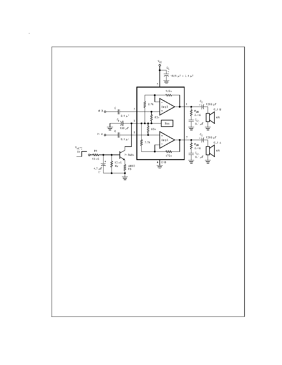
Typical Application
Connection Diagram
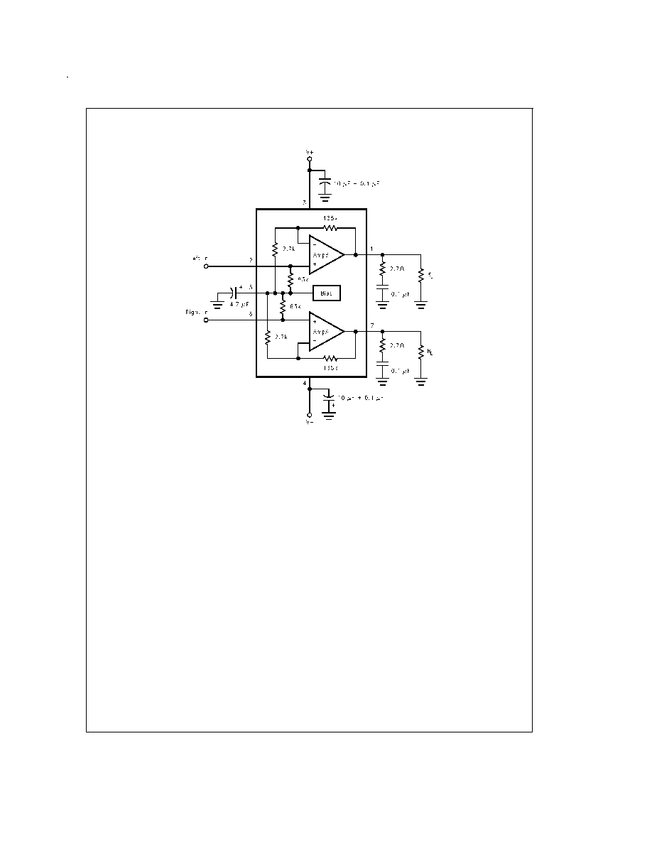
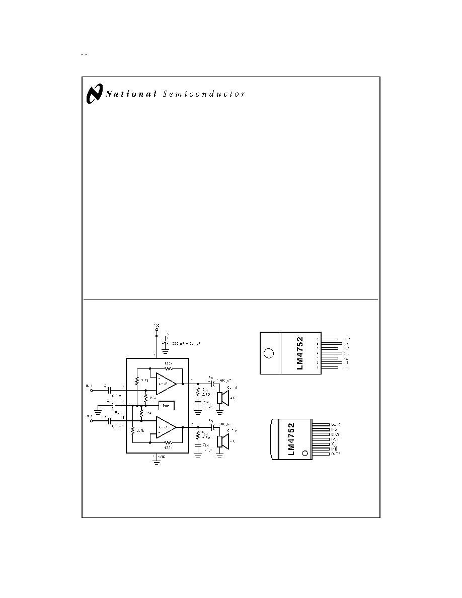
DS100039-1
FIGURE 1. Typical Audio Amplifier Application Circuit
Plastic Package
DS100039-2
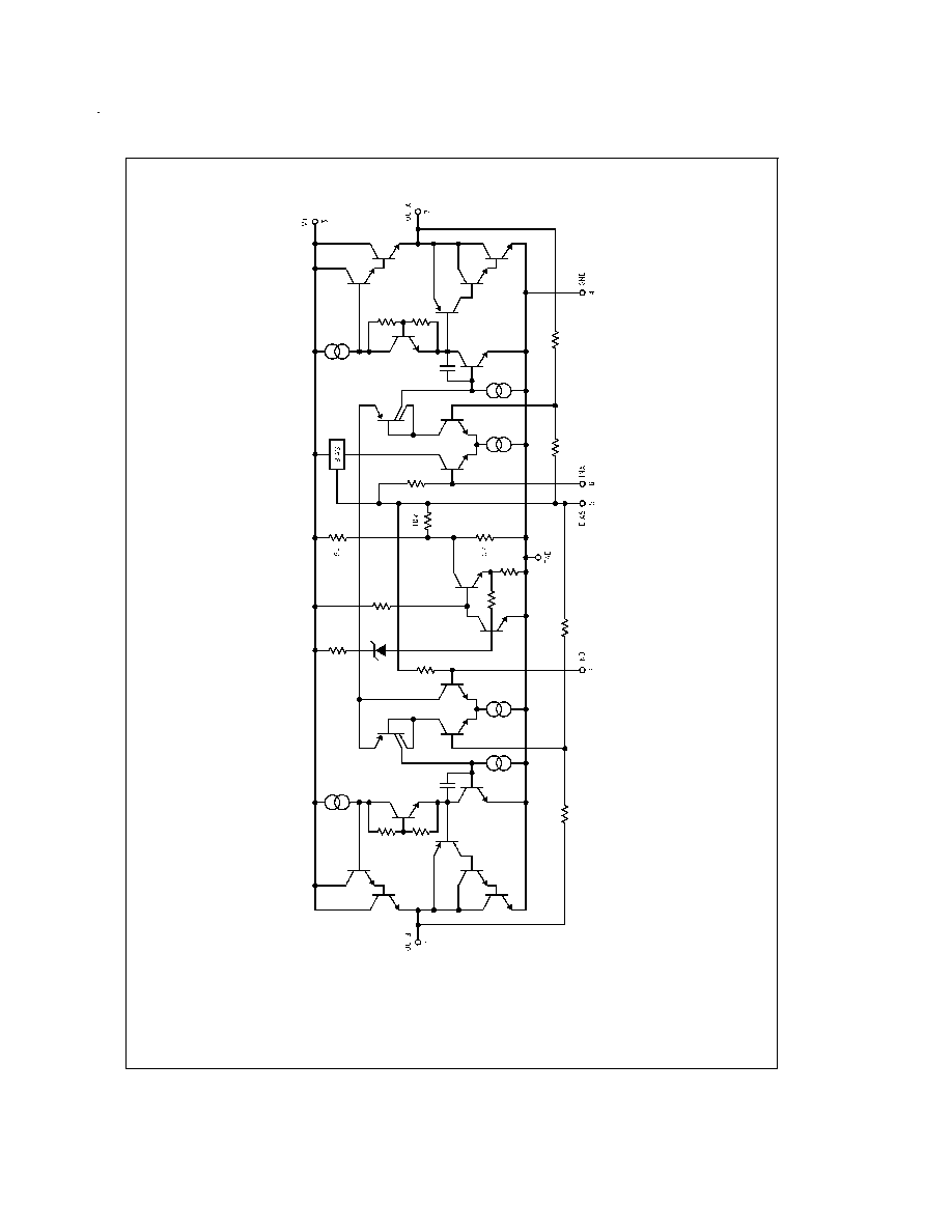
Package Description
Top View
Order Number LM4752T
Package Number TA07B
DS100039-50
Package Description
Top View
Order Number LM4752TS
Package Number TS07B
February 1999
LM4752
Stereo
1
1
W
Audio
Power
Amplifier
© 1999 National Semiconductor Corporation
DS100039
www.national.com
Absolute Maximum Ratings
(Note 2)
If Military/Aerospace specified devices are required,
please contact the National Semiconductor Sales Office/
Distributors for availability and specifications.
Supply Voltage
40V
Input Voltage
±
0.7V
Output Current
Internally Limited
Power Dissipation (Note 3)
62.5W
ESD Susceptability (Note 4)
2 kV
Junction Temperature
150∞C
Soldering Information
T Package (10 sec)
250∞C
Storage Temperature
-40∞C to 150∞C
Operating Ratings
Temperature Range
T
MIN
T
A
T
MAX
-40∞C
T
A
+85∞C
Supply Voltage
9V to 32V
JC
2∞C/W
JA
79∞C/W
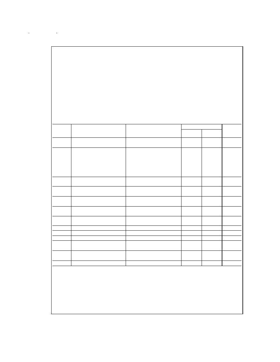
Electrical Characteristics
The following specifications apply to each channel with V
CC
= 24V, T
A
= 25∞C unless otherwise specified.
Symbol
Parameter
Conditions
LM4752
Units
(Limits)
Typical
(Note 5)
Limit
(Note 6)
I
total
Total Quiescent Power Supply
Current
V
INAC
= 0V, V
o
= 0V, R
L
=
10.5
20
mA(max)
7
mA(min)
P
o
Output Power (Continuous
f = 1 kHz, THD+N = 10%, R
L
= 8
7
W
Average per Channel)
f = 1 kHz, THD+N = 10%, R
L
= 4
10
W(min)
V
CC
= 20V, R
L
= 8
4
W
V
CC
= 20V, R
L
= 4
7
W
f = 1 kHz, THD+N = 10%, R
L
= 4
V
S
= 12V, TO-263 Pkg.
2.5
W
THD+N
Total Harmonic Distortion plus
Noise
f = 1 kHz, P
o
= 1 W/ch, R
L
= 8
0.08
%
V
OSW
Output Swing
R
L
= 8
, V
CC
= 20V
15
V
R
L
= 4
, V
CC
= 20V
14
V
X
talk
Channel Separation
See
Figure 1
55
dB
f = 1 kHz, V
o
= 4 Vrms, R
L
= 8
PSRR
Power Supply Rejection Ratio
See
Figure 1
50
dB
V
CC
= 22V to 26V, R
L
= 8
V
ODV
Differential DC Output Offset
Voltage
V
INAC
= 0V
0.09
0.4
V(max)
SR
Slew Rate
2
V/µs
R
IN
Input Impedance
83
k
PBW
Power Bandwidth
3 dB BW at P
o
= 2.5W, R
L
= 8
65
kHz
A
VCL
Closed Loop Gain (Internally Set)
R
L
= 8
34
33
dB(min)
35
dB(max)
e
in
Noise
IHF-A Weighting Filter, R
L
= 8
0.2
mVrms
Output Referred
I
o
Output Short Circuit Current Limit
V
IN
= 0.5V, R
L
= 2
2
A(min)
Note 1: All voltages are measured with respect to the GND pin (4), unless otherwise specified.
Note 2:
Absolute Maximum Ratings indicate limits beyond which damage to the device may occur. Operating Ratings indicate conditions for which the device is func-
tional, but do not guarantee specific performance limits.
Electrical Characteristics state DC and AC electrical specifications under particular test conditions which guar-
antee specific performance limits. This assumes that the device is within the Operating Ratings. Specifications are not guaranteed for parameters where no limit is
given, however, the typical value is a good indication of device performance.
Note 3: For operating at case temperatures above 25∞C, the device must be derated based on a 150∞C maximum junction temperature and a thermal resistance of
JC
= 2∞C/W (junction to case). Refer to the section Determining the Maximum Power Dissipation in the Application Information section for more information.
Note 4: Human body model, 100 pF discharged through a 1.5 k
resistor.
Note 5: Typicals are measured at 25∞C and represent the parametric norm.
Note 6: Limits are guarantees that all parts are tested in production to meet the stated values.
Note 7: The TO-263 Package is not recommended for V
S
>
16V due to impractical heatsinking limitations.
www.national.com
2