 | –≠–ª–µ–∫—Ç—Ä–æ–Ω–Ω—ã–π –∫–æ–º–ø–æ–Ω–µ–Ω—Ç: LM4753 | –°–∫–∞—á–∞—Ç—å:  PDF PDF  ZIP ZIP |
LM4753
Dual 10W Audio Power Amplifier w/Mute, Standby and
Volume Control
General Description
The LM4753 is a stereo audio amplifier capable of delivering
10W/channel at 10% distortion into a 8
load. The power
amp has an internally set gain of 30 dB. A 0V≠5V DC con-
trolled volume block provides 80 dB of attenuation from input
to line-out. Line outputs are available after the volume con-
trol for signal routing.
The amplifier has a smooth transition fade-in/out mute and a
power conserving standby function which are controlled
through TTL or CMOS logic. Both functions provide over
75 dB of attenuation.
The LM4753 maintains an excellent Signal-to-Noise ratio of
greater than 70 dB with a low noise floor less than 2 mV. The
IC also maintains above 50 dB of channel separation.
The LM4753 is available in a 15-lead non-isolated plastic
package and is designed for use in TV applications requiring
single supply operation.
Key Specifications
n
Output power into 8
at 10% THD
10W
n
Maximum operating voltage
28V
n
Power output stage Noise floor
2 mV
n
Line output Noise floor
55 µV
n
0V≠5V DC controlled volume attenuation
80 dB
n
Mute attenuation
75 dB
n
Standby-mode supply current
7 mA
Features
n
Quiet fade-in/out mute function
n
Stereo variable line-out pins
n
AC output short circuit protection
n
Thermal shutdown protection
Applications
n
Stereo TVs
n
Component stereo
n
Compact stereo
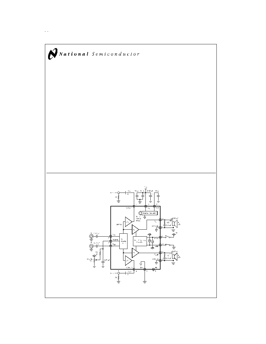
Typical Application
DS100043-1
FIGURE 1. Typical Audio Amplifier Application Circuit
June 1999
LM4753
Dual
10W
Audio
Power
Amplifier
w/Mute,
Standby
and
V
olume
Control
© 1999 National Semiconductor Corporation
DS100043
www.national.com
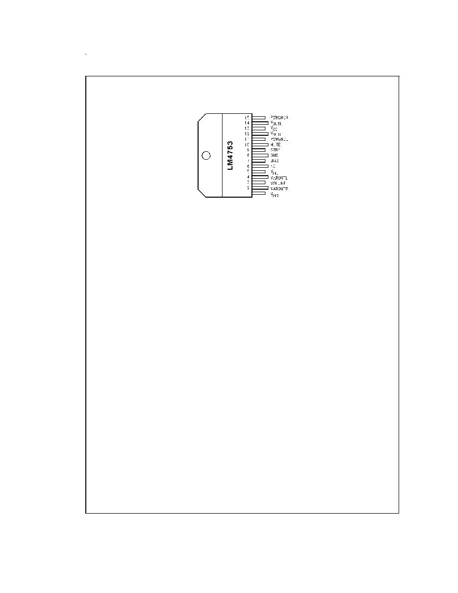
Connection Diagram
Plastic Package
DS100043-2
Top View
Order Number
See NS Package Number TA15A for
Staggered Lead Non-Isolated Package
www.national.com
2
Absolute Maximum Ratings
(Notes 3, 4)
If Military/Aerospace specified devices are required,
please contact the National Semiconductor Sales Office/
Distributors for availability and specifications.
Supply Voltage
32V
Output Current
Internally Limited
Power Dissipation (Note 5)
22W
ESD Susceptibility (Note 6)
2000V
ESD Susceptibility (Note 7)
250V
Junction Temperature
150∞C
Soldering Information
T Package (10 sec)
260∞C
Storage Temperature
-40∞C to +150∞C
Input Signal Voltage Range
±
3V
Operating Ratings
(Notes 3, 4)
Temperature Range
T
MIN
T
A
T
MAX
-40∞C
T
A
+85∞C
Supply Voltage
15V to 28V
JA
(Junction to Ambient)
35∞C/W
JC
(Junction to Case)
1.5∞C/W
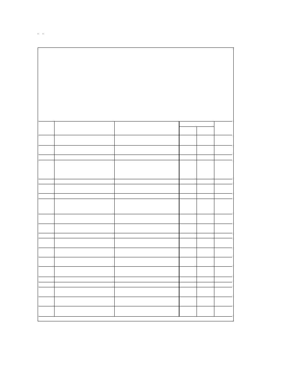
Electrical Characteristics
(Notes 3, 4)
The following specifications apply for V
CC
= +22V, and Volume
@
0 dB unless otherwise specified. Limits apply for T
A
= 25∞C.
Symbol
Parameter
Conditions
LM4753
Units
(Limits)
Typical
(Note 8)
Limit
(Note 9)
I
CQ
(Note 1)
Total Quiescent Power Supply
Current
V
CM
= 0V, V
o
= 0V, I
o
= 0 mA
20
mA (min)
80
140
mA (max)
I
STBY
(Note 1)
Standby Current
V
STDBY
= 5V, Standby-on
7
10
mA (max)
I
MUTE
Mute Current
V
MUTE
= 5V Mute-on
13
20
mA
A
M
(Note 2)
Mute Attenuation
V
MUTE
= 5V, V
STDBY
= 0V. Mute-on
Signal Input
75
60
dB (min)
V
MUTE
= 0V. V
STDBY
= 0V. Mute-off
2 Vrms
±
5
dB
Volume Attenuation Range
80
70
dB (min)
Volume Absolute Attenuation
Line-out
Pin 3
@
0V = 80 dB, 2V = 14 dB,
3V = 8 dB, 4V = 3 dB, 5V = 0 dB
±
3
±
5
dB (max)
Line-out Offset Voltage
20
40
mV (max)
P
O
(Note 1)
Output Power (Continuous Average)
THD+N = 10% (max)
f = 1 kHz, R
L
= 8
, V
CC
= 28
11.8
W
f = 1 kHz, R
L
= 8
, V
CC
= 22V
7
6.5
W(min)
THD+N
(Note 2)
Total Harmonic Distortion Plus Noise
P
o
= 1W, f = 1 kHz, R
L
= 8
0.4
1
% (max)
Xtalk
(Note 2)
Channel Separation
f = 1 kHz, P
o
= 5W, R
L
= 8
50
dB
Power Amp Closed-Loop Gain Error
Internal Gain = 30 dB
0.5
±
1
dB (max)
SR
(Note 2)
Slew Rate
V
IN
= 100 mVp-p, t
RISE
= 2 ns, R
L
= 8
3
V/µs
R
IN
(Note 1)
Input Impedance
32
k
I
O
(Note 1)
Output Current Limit
V
IN
= 100 mV DC, t
ON
= 1 ms, R
L
= 1
2.5
2.0
A(min)
PSRR
(Note 2)
Power Supply Rejection Ratio
Vpin 13 AC = 1 Vrms, f = 100 Hz
50
dB
V
CM
= 0V, I
o
= 0 mA
GBWP
Gain-Bandwidth Product
f
o
= 100 kHz, V
IN
= 50 mvrms
2
MHz
Power Bandwidth
-3 dB Bandwidth at 5W
90
kHz
eVCA
out
VCA Output Noise
IHF - A Weighting Filter
R
IN
= 25
55
µV
e
out
Power Amp Output Noise
IHF - A Weighting Filter
R
IN
= 25
1.8
mV
SNR
Signal-to-Noise Ratio
Measured at 1 kHz, R
s
= 25
P
o
= 4.8W, A - Weighted,
70
dB
www.national.com
3
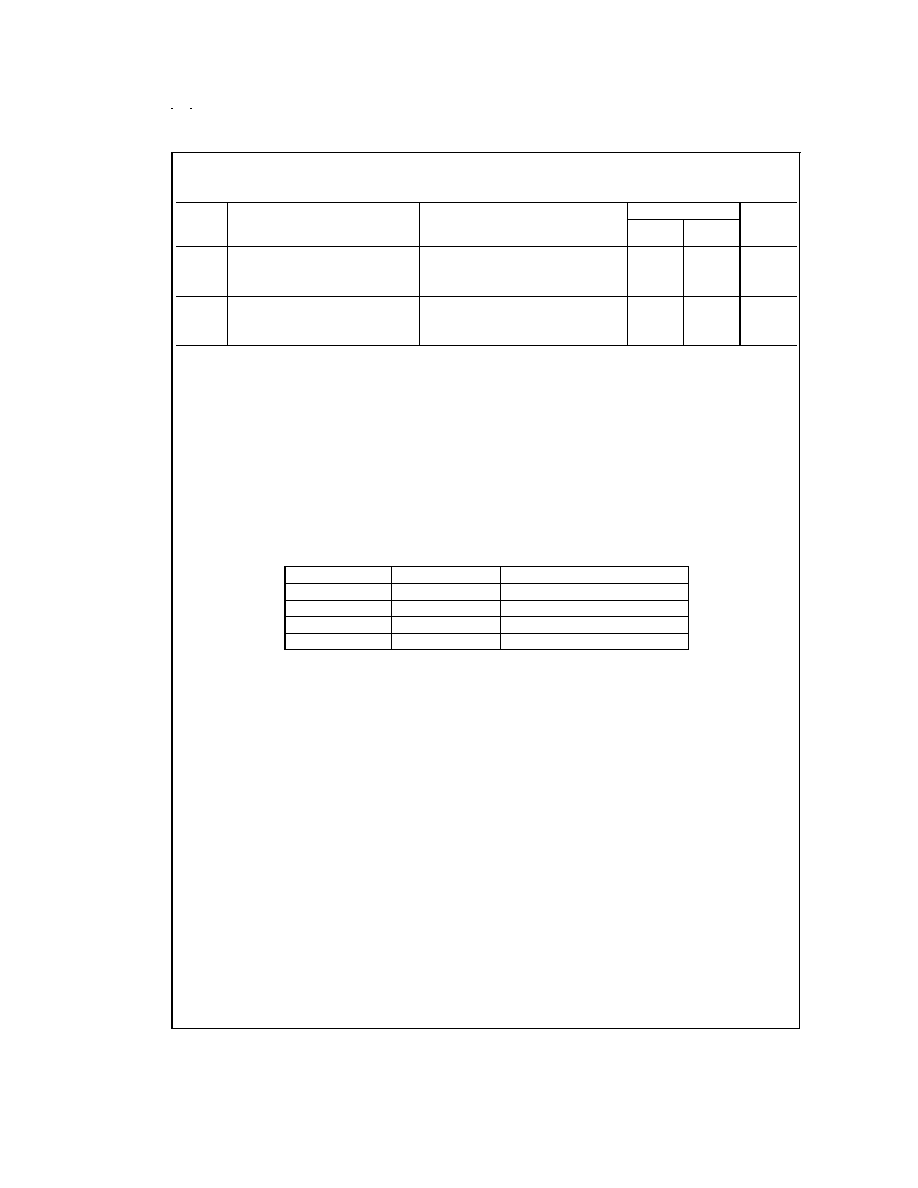
Electrical Characteristics
(Notes 3, 4) (Continued)
The following specifications apply for V
CC
= +22V, and Volume
@
0 dB unless otherwise specified. Limits apply for T
A
= 25∞C.
Symbol
Parameter
Conditions
LM4753
Units
(Limits)
Typical
(Note 8)
Limit
(Note 9)
Standby
V
IL
Standby Low Input Voltage
0.8
V (max)
V
IH
Standby High Input Voltage
2.0
V (min)
Mute
V
IL
Mute Low Input Voltage
0.8
V (max)
V
IH
Mute High Input Voltage
2.0
V (min)
Note 1: DC Electrical Test.
Note 2: AC Electrical Test.
Note 3: Absolute Maximum Ratings indicate limits beyond which damage to the device may occur. Operating Ratings indicate conditions for which the device is
functional, but do not guarantee specific performance limits. Electrical Characteristics state DC and AC electrical specifications under particular test conditions
which guarantee specific performance limits. This assumes that the device is within the Operating Ratings. Specifications are not guaranteed for parameters where
no limit is given, however, the typical value is a good indication of device performance.
Note 4: All voltages are measured with respect to the ground (pin 8), unless otherwise specified.
Note 5: The maximum power dissipation must be derated at elevated temperatures and is dictated by T
JMAX
,
JA
, and the ambient temperature, T
A
. The maximum
allowable power dissipation is PDMAX = (T
JMAX
- T
A
)/
JA
or the number given in the Absolute Maximum Ratings, whichever is lower. For operating at case tempera-
tures above 25∞C, the device must be derated based on a 150∞C maximum junction temperature and a thermal resistance of
JC
= 5∞C/W (junction to case).
Note 6: Human body model, 100 pF discharged through a 1.5 k
resistor.
Note 7: Machine model, 200 pF≠240 pF discharge through all pins.
Note 8: Typicals are measured at 25∞C and represent the parametric norm.
Note 9: Limits are guarantees that all parts are tested in production to meet the stated values.
Standby Mute Pin Function Table
Standby (Pin 9)
Mute (Pin 10)
Operating Condition
"L" or Open
"L"
Play
"L" or Open
"H" or Open
Mute
"H"
"L"
Standby
"H"
"H" or Open
Standby
www.national.com
4
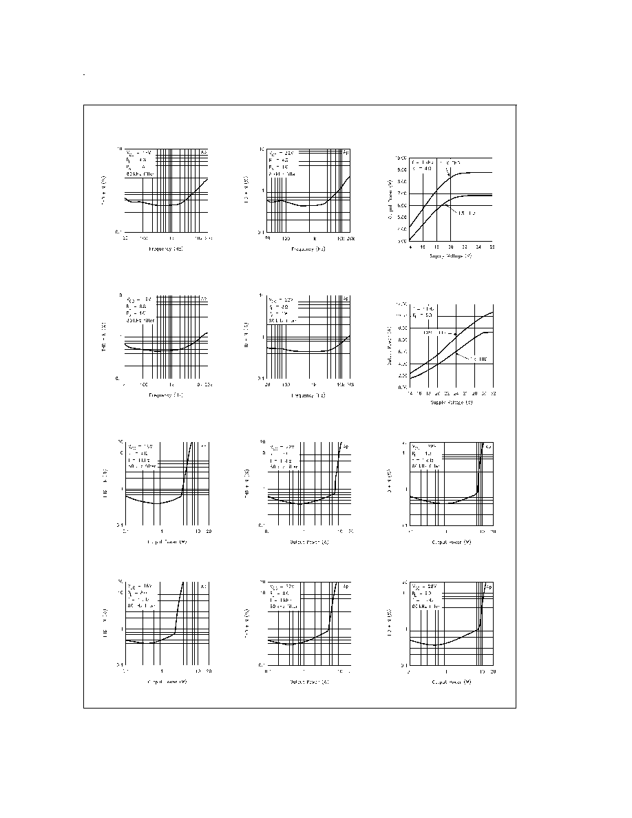
Typical Performance Characteristics
THD+N vs Frequency
DS100043-8
THD+N vs Frequency
DS100043-9
Output Power vs
Supply Voltage
DS100043-10
THD+N vs Frequency
DS100043-11
THD+N vs Frequency
DS100043-12
Output Power vs
Supply Voltage
DS100043-13
THD+N vs Output Power
DS100043-14
THD+N vs Output Power
DS100043-15
THD+N vs Output Power
DS100043-16
THD+N vs Output Power
DS100043-17
THD+N vs Output Power
DS100043-18
THD+N vs Output Power
DS100043-19
www.national.com
5