LM4755
Stereo 11W Audio Power Amplifier with Mute
General Description
The LM4755 is a stereo audio amplifier capable of delivering
11W per channel of continuous average output power to a
4
load or 7W per channel into 8
using a single 24V supply
at 10% THD+N. The internal mute circuit and pre-set gain re-
sistors provide for a very economical design solution.
Output power specifications at both 20V and 24V supplies
and low external component count offer high value to con-
sumer electronic manufacturers for stereo TV and compact
stereo applications. The LM4755 is specifically designed for
single supply operation.
Key Specifications
n
Output power at 10% THD with 1 kHz into 4
at V
CC
=
24V
11W(typ)
n
Output power at 10% THD with 1 kHz into 8
at V
CC
=
24V
7W(typ)
n
Closed loop gain
34 dB(typ)
n
P
O
at 10% THD
@
1 kHz into 4
single-ended TO-263
pkg. at V
CC
=12V 2.5W(typ)
n
P
O
at 10% THD
@
1 kHz into 8
bridged TO-263 pkg.
at V
CC
=12V 5W(typ)
Features
n
Drives 4
and 8
loads
n
Integrated mute function
n
Internal Gain Resistors
n
Minimal external components needed
n
Single supply operation
n
Internal current limiting and thermal protection
n
Compact 9-lead TO-220 package
Applications
n
Stereos TVs
n
Compact stereos
n
Mini component stereos
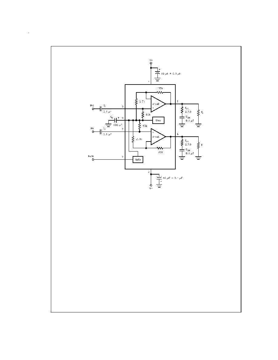
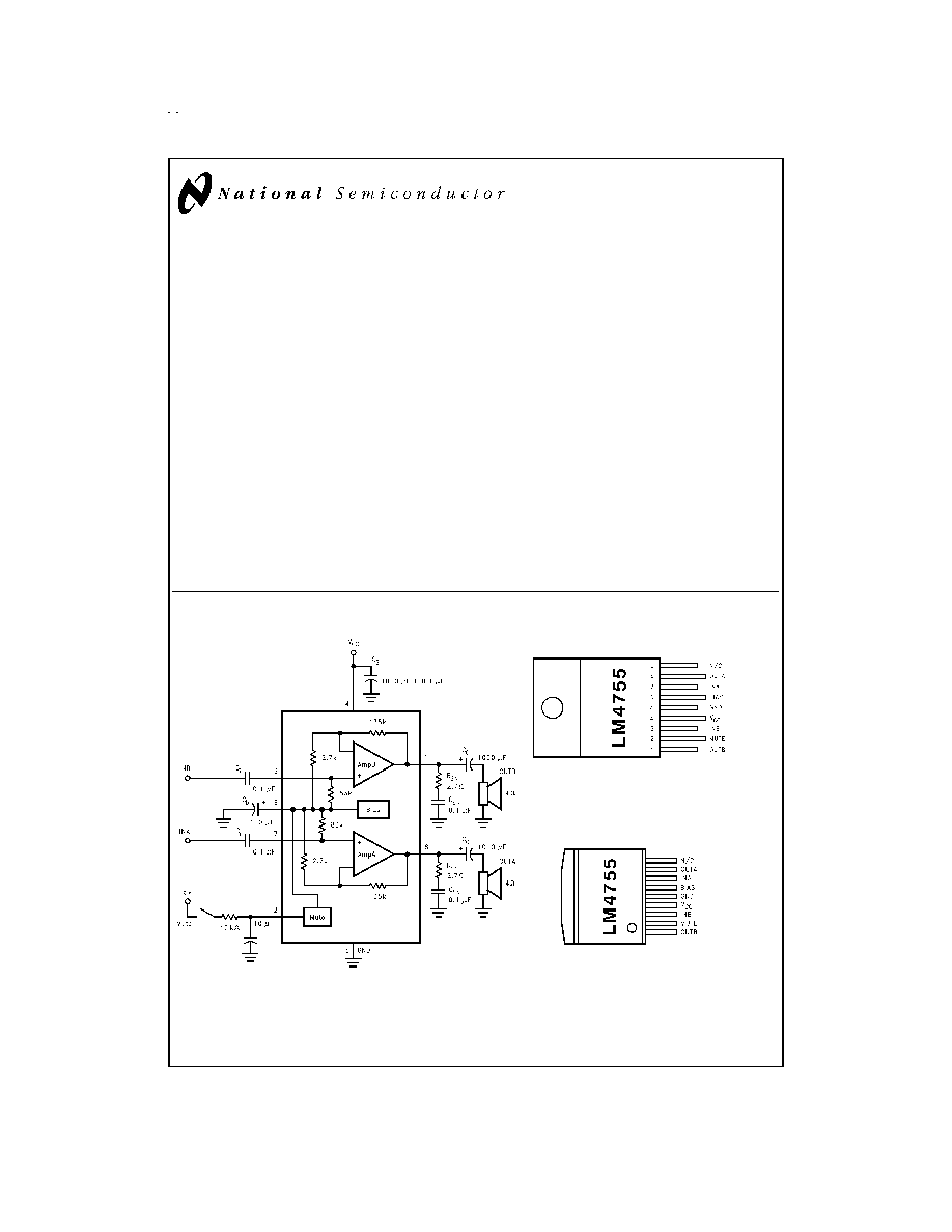
Typical Application
Connection Diagrams
DS100059-1
FIGURE 1. Typical Audio Amplifier Application Circuit
Plastic Package
DS100059-2
Package Description
Top View
Order Number LM4755T
Package Number TA09A
DS100059-36
Top View
Order Number LM4755TS
Package Number TS9A
February 1999
LM4755
Stereo
1
1
W
Audio
Power
Amplifier
with
Mute
© 1999 National Semiconductor Corporation
DS100059
www.national.com
Absolute Maximum Ratings
(Note 2)
If Military/Aerospace specified devices are required,
please contact the National Semiconductor Sales Office/
Distributors for availability and specifications.
Supply Voltage
40V
Input Voltage
±
0.7V
Output Current
Internally Limited
Power Dissipation (Note 3)
62.5W
ESD Susceptability (Note 4)
2 kV
Junction Temperature
150∞C
Soldering Information
T Package (10 seconds)
250∞C
Storage Temperature
-40∞C to 150∞C
Operating Ratings
Temperature Range
T
MIN
T
A
T
MAX
-40∞C
T
A
+85∞C
Supply Voltage
9V to 32V
JC
2∞C/W
JA
76∞C/W
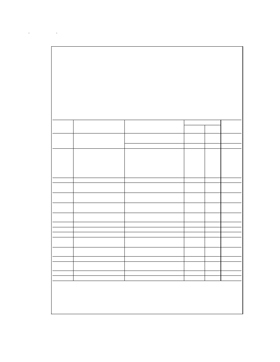
Electrical Characteristics
The following specifications apply to each channel with V
CC
= 24V, T
A
= 25∞C unless otherwise specified.
Symbol
Parameter
Conditions
LM4755
Units
(Limits)
Typical
(Note 5)
Limit
I
TOTAL
Total Quiescent Power
Supply Current
Mute Off
10
15
mA(max)
7
mA(min)
Mute On
7
mA
P
O
Output Power (Continuous
Average per Channel)
f = 1 kHz, THD+N = 10%, R
L
= 8
7
W
f = 1 kHz, THD+N = 10%, R
L
= 4
11
10
W(min)
V
S
= 20V, R
L
= 8
4
W
V
S
= 20V, R
L
= 4
7
W
f = 1 kHz, THD+N = 10%, R
L
= 4
V
S
= 12V, TO-263 Pkg.
2.5
W
THD
Total Harmonic Distortion
f = 1 kHz, P
O
= 1 W/ch, R
L
= 8
0.08
%
V
OSW
Output Swing
P
O
= 10W, R
L
= 8
15
V
P
O
= 10W, R
L
= 4
14
V
X
TALK
Channel Separation
See Apps. Circuit
55
dB
f = 1 kHz, V
O
= 4 Vrms
PSRR
Power Supply Rejection Ratio
See Apps. Circuit
50
dB
f = 120 Hz, V
O
= 1 mVrms
V
ODV
Differential DC Output Offset
Voltage
V
IN
= 0V
0.09
0.4
V(max)
SR
Slew Rate
2
V/µs
R
IN
Input Impedance
83
k
PBW
Power Bandwidth
3 dB BW at P
O
= 2.5W, R
L
= 8
65
kHz
A
VCL
Closed Loop Gain
(Internally Set)
R
L
= 8
34
33
dB(min)
35
dB(max)
e
IN
Noise
IHF-A Weighting Filter, R
L
= 8
Output Referred
0.2
mVrms
I
O
Output Short Circuit Limit
V
IN
= 0.5V, R
L
= 2
2
A(min)
Mute Pin
V
IL
Mute Low Input Voltage
Not in Mute Mode
0.8
V(max)
V
IH
Mute High Input Voltage
In Mute Mode
2.0
2.5
V(min)
A
M
Mute Attenuation
V
MUTE
= 5.0V
80
dB
Note 1: All voltages are measured with respect to the GND pin (5), unless otherwse specified.
Note 2: Absolute Maximum Ratings indicate limits beyond which damage to the device may occur. Operating Ratings indicate conditions for which the device is func-
tional, but do not guarantee specific performance limits. Electrical Characteristics state DC and AC electrical specifications under particular test conditions which guar-
antee specific performance limits. This assumes that the device is within the Operating Ratings. Specifications are not guaranteed for parameters where no limit is
given, however, the typical value is a good indication of device performance.
Note 3: For operating at case temperatures above 25∞C, the device must be derated based on a 150∞C maximum junction temperature and a thermal resistance of
JC
= 2∞C/W (junction to case). Refer to the section Determining the Maximum Power Dissipation in the Application Information section for more information.
Note 4: Human body model, 100 pF discharged through a 1.5 k
resistor.
www.national.com
2
Electrical Characteristics
(Continued)
Note 5: Typicals are measured at 25∞C and represent the parametric norm.
Note 6: Limits are guaranteed that all parts are tested in production to meet the stated values.
Note 7: The TO-263 Package is not recommended for V
S
>
16V due to impractical heatsinking limitations.
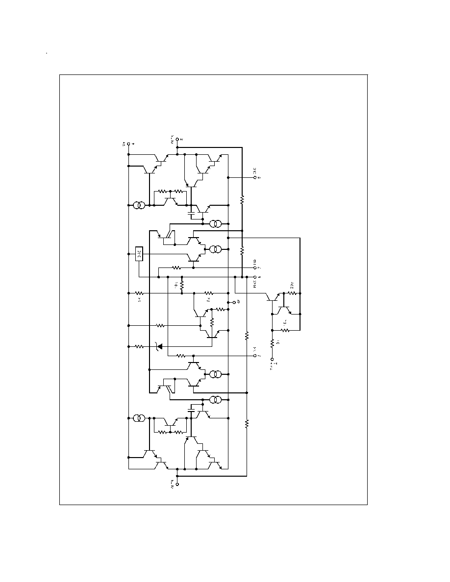
Equivalent Schematic
DS100059-3
www.national.com
3
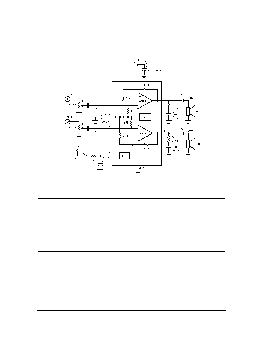
System Application Circuit
External Components Description
Components
Function Description
1, 2
C
S
Provides power supply filtering and bypassing.
3, 4
R
SN
Works with C
SN
to stabilize the output stage from high frequency oscillations.
5, 6
C
SN
Works with R
SN
to stabilize the output stage from high frequency oscillations.
7
C
b
Provides filtering for the internally generated half-supply bias generator.
8, 9
C
i
Input AC coupling capacitor which blocks DC voltage at the amplifier's input terminals. Also creates a
high pass filter with fc=1/(2
∑
∑ Rin ∑ Cin).
10, 11
C
o
Output AC coupling capacitor which blocks DC voltage at the amplifier's output terminal. Creates a high
pass filter with fc=1/(2
∑
∑ Rout ∑ Cout).
12, 13
R
i
Voltage control - limits the voltage level allowed to the amplifier's input terminals.
14
R
m
Works with C
m
to provide mute function timing.
15
C
m
Works with R
m
to provide mute function timing.
DS100059-5
FIGURE 3. Circuit for External Components Description
www.national.com
5