 | –≠–ª–µ–∫—Ç—Ä–æ–Ω–Ω—ã–π –∫–æ–º–ø–æ–Ω–µ–Ω—Ç: LM4780TA | –°–∫–∞—á–∞—Ç—å:  PDF PDF  ZIP ZIP |

LM4780 Overture
TM
Audio Power Amplifier Series
Stereo 60W, Mono 120W Audio Power Amplifier with
Mute
General Description
The LM4780 is a stereo audio amplifier capable of typically
delivering 60W per channel of continuous average output
power into an 8
load with less than 0.5% THD+N from
20Hz - 20kHz.
The LM4780 is fully protected utilizing National's Self Peak
Instantaneous Temperature (∞Ke) (SPiKe
TM
) protection cir-
cuitry. SPiKe provides a dynamically optimized Safe Operat-
ing Area (SOA). SPiKe protection completely safeguards the
LM4780's outputs against over-voltage, under-voltage, over-
loads, shorts to the supplies or GND, thermal runaway and
instantaneous temperature peaks. The advanced protection
features of the LM4780 places it in a class above discrete
and hybrid amplifiers.
Each amplifier of the LM4780 has an independent smooth
transition fade-in/out mute.
The LM4780 can easily be configured for bridge or parallel
operation for 120W mono solutions.
Key Specifications
n
Output Power/Channel with 0.5% THD+N, 1kHz into
8
60W (typ)
n
THD+N at 2 x 30W into 8
(20Hz - 20kHz) 0.03% (typ)
n
THD+N at 2 x 30W into 6
(20Hz - 20kHz) 0.05% (typ)
n
THD+N at 2 x 30W into 4
(20Hz - 20kHz) 0.07% (typ)
n
Mute Attenuation
110dB (typ)
n
PSRR
85dB (min)
n
Slew Rate
19V/µs (typ)
Features
n
SPiKe Protection
n
Low external component count
n
Quiet fade-in/out mute mode
n
Wide supply range: 20V - 84V
n
Signal-to-Noise Ratio
97dB (ref. to P
O
= 1W)
Applications
n
Audio amplifier for component stereo
n
Audio amplifier for compact stereo
n
Audio amplifier for self-powered speakers
n
Audio amplifier for high-end and HD TVs
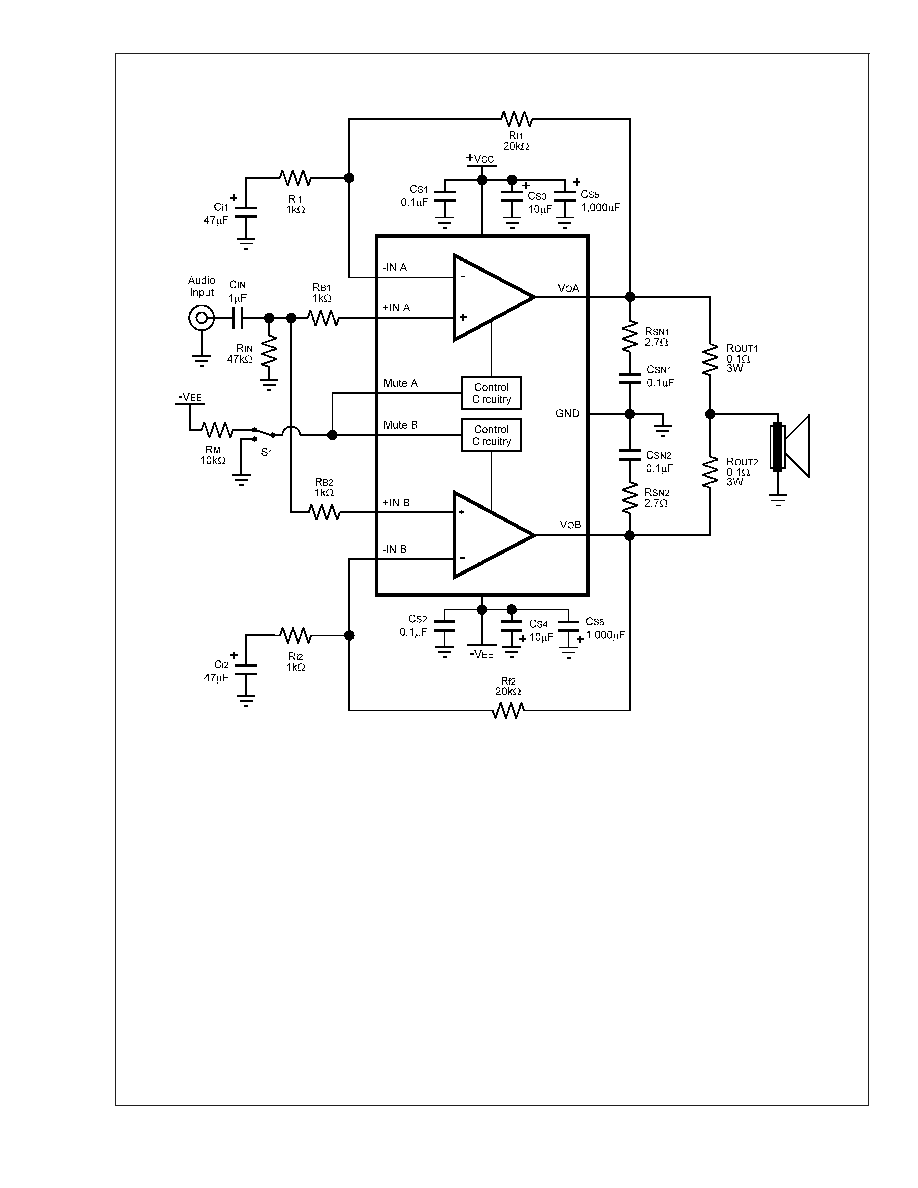
Typical Application
SPiKe
TM
Protection and Overture
TM
are trademarks of National Semiconductor Corporation.
20058622
FIGURE 1. Typical Audio Amplifier Application Circuit
July 2003
LM4780
Overture
TM
Audio
Power
Amplifier
Series
Stereo
60W
,
Mono
120W
Audio
Power
Amplifier
with
Mute
© 2003 National Semiconductor Corporation
DS200586
www.national.com
Connection Diagrams
Plastic Package (Note 14)
200586D6
Top View
Order Number LM4780TA
See NS Package Number TA27A
TO-220 Top Marking
200586A2
Top View
U - Wafer Fab Code
Z - Assemble Plant Code
XY - Date Code
TT - Die Run Traceability
L4780TA - LM4780TA
LM4780
www.national.com
2
Absolute Maximum Ratings
(Notes 1,
2)
If Military/Aerospace specified devices are required,
please contact the National Semiconductor Sales Office/
Distributors for availability and specifications.
Supply Voltage |V
+
| + |V
-
|
(No Signal)
94V
Supply Voltage |V
+
| + |V
-
|
(Input Signal)
84V
Common Mode Input Voltage
(V
+
or V
-
) and
|V
+
| + |V
-
|
80V
Differential Input Voltage (Note 13)
60V
Output Current
Internally Limited
Power Dissipation (Note 3)
125W
ESD Susceptability (Note 4)
3.0kV
ESD Susceptability (Note 5)
200V
Junction Temperature (T
JMAX
) (Note 9)
150∞C
Soldering Information
TA Package (10 seconds)
260∞C
Storage Temperature
-40∞C to +150∞C
Thermal Resistance
JA
30∞C/W
JC
0.8∞C/W
Operating Ratings
(Notes 1, 2)
Temperature Range
T
MIN
T
A
T
MAX
-20∞C
T
A
+85∞C
Supply Voltage |V
+
| + |V
-
|
20V
V
TOTAL
84V
Note: Operation is guaranteed up to 84V; however, distor-
tion may be introduced from SPiKe protection circuitry if
proper thermal considerations are not taken into account.
Refer to the Thermal Considerations section for more
information.
Electrical Characteristics
(Notes 1, 2)
The following specifications apply for V
+
= +35V, V
-
= -35V, I
MUTE
= -1mA and R
L
= 8
unless otherwise specified. Limits ap-
ply for T
A
= 25∞C.
Symbol
Parameter
Conditions
LM4780
Units
(Limits)
Typical
Limit
(Note 6)
(Notes 7, 8)
|V
+
| + |V
-
|
Power Supply Voltage (Note
10)
GND - V
-
9V
18
20
84
V (min)
V (max)
A
M
Mute Attenuation
I
MUTE
= 0mA
110
80
dB (min)
P
O
Output Power (RMS)
THD+N = 0.5% (max)
f = 1kHz; f = 20kHz
|V
+
| = |V
-
| = 25V, R
L
= 4
|V
+
| = |V
-
| = 30V, R
L
= 6
|V
+
| = |V
-
| = 35V, R
L
= 8
55
55
60
50
50
50
W (min)
W (min)
W (min)
THD+N
Total Harmonic Distortion +
Noise
P
O
= 30W, f = 20Hz - 20kHz
A
V
= 26dB
|V
+
| = |V
-
| = 25V, R
L
= 4
|V
+
| = |V
-
| = 30V, R
L
= 6
|V
+
| = |V
-
| = 35V, R
L
= 8
0.07
0.05
0.03
%
%
%
X
talk
Channel Separation (Note 11)
P
O
= 10W, f = 1kHz
70
dB
P
O
= 10W, f = 10kHz
72
dB
SR
Slew Rate
V
IN
= 2.0V
P-P
, t
RISE
= 2ns
19
8
V/µs (min)
I
DD
Total Quiescent Power
V
CM
= 0V,
110
170
mA (max)
Supply Current
V
O
= 0V, I
O
= 0A
V
OS
Input Offset Voltage
V
CM
= 0V, I
O
= 0mA
1
10
mV (max)
I
B
Input Bias Current
V
CM
= 0V, I
O
= 0mA
0.2
1
µA (max)
I
O
Output Current Limit
|V
+
| = |V
-
| = 20V, t
ON
= 10ms
11.5
7
A (min)
V
OD
Output Dropout Voltage
(Note 12)
|V
+
- V
O
|, V
+
= 28V, I
O
= +100mA
|V
-
- V
O
|, V
-
= -28V, I
O
= -100mA
1.6
2.5
2.0
3.0
V (max)
V (max)
PSRR
Power Supply Rejection Ratio
(Note 15)
V
+
= 40V to 20V, V
-
= -40V,
V
CM
= 0V, I
O
= 0mA
120
85
dB (min)
V
+
= 40V, V
-
= -40V to -20V,
V
CM
= 0V, I
O
= 0mA
105
85
dB (min)
CMRR
Common Mode Rejection Ratio
(Note 15)
V
+
= 60V to 20V, V
-
= -20V to -60V,
V
CM
= 20V to -20V, I
O
= 0mA
110
85
dB (min)
LM4780
www.national.com
3
Electrical Characteristics
(Notes 1, 2) (Continued)
The following specifications apply for V
+
= +35V, V
-
= -35V, I
MUTE
= -1mA and R
L
= 8
unless otherwise specified. Limits ap-
ply for T
A
= 25∞C.
Symbol
Parameter
Conditions
LM4780
Units
(Limits)
Typical
Limit
(Note 6)
(Notes 7, 8)
A
VOL
Open Loop Voltage Gain
R
L
= 2k
, V
O
= 40V
115
90
dB (min)
GBWP
Gain Bandwidth Product
f
IN
= 100kHz, V
IN
= 50mV
RMS
8
2
MHz (min)
e
IN
Input Noise
IHF-A-Weighting Filter,
R
IN
= 600
(Input Referred)
2.0
10
µV (max)
SNR
Signal-to-Noise Ratio
P
O
= 1W
RMS
; A-Weighted Filter
f
IN
= 1kHz, R
S
= 25
97
dB
P
O
= 50W
RMS
; A-Weighted Filter
f
IN
= 1kHz, R
S
= 25
114
dB
IMD
Intermodulation Distortion
60Hz, 7kHz, 4:1 (SMPTE)
60Hz, 7kHz, 1:1 (SMPTE)
0.004
0.009
%
%
Note 1: All voltages are measured with respect to the ground pins, unless otherwise specified.
Note 2: Absolute Maximum Ratings indicate limits beyond which damage to the device may occur. Operating Ratings indicate conditions for which the device is
functional, but do not guarantee specific performance limits. Electrical Characteristics state DC and AC electrical specifications under particular test conditions which
guarantee specific performance limits. This assumes that the device is within the Operating Ratings. Specifications are not guaranteed for parameters where no limit
is given; however, the typical value is a good indication of device performance.
Note 3: The maximum power dissipation must be de-rated at elevated temperatures and is dictated by T
JMAX
,
JC
, and the ambient temperature T
A
. The maximum
allowable power dissipation is P
DMAX
= (T
JMAX
-T
A
)/
JC
or the number given in the Absolute Maximum Ratings, whichever is lower. For the LM4780, T
JMAX
= 150∞C
and the typical
JC
is 0.8∞C/W. Refer to the Thermal Considerations section for more information.
Note 4: Human body model, 100pF discharged through a 1.5k
resistor.
Note 5: Machine Model: a 220pF - 240pF discharged through all pins.
Note 6: Typical specifications are measured at 25∞C and represent the parametric norm.
Note 7: Tested limits are guaranteed to National's AOQL (Average Outgoing Quality Level).
Note 8: Datasheet min/max specification limits are guaranteed by design, test, or statistical analysis.
Note 9: The maximum operating junction temperature is 150∞C. However, the instantaneous Safe Operating Area temperature is 250∞C.
Note 10: V
-
must have at least - 9V at its pin with reference to GND in order for the under-voltage protection circuitry to be disabled. In addition, the voltage
differential between V
+
and V
-
must be greater than 14V.
Note 11: Cross talk performance was measured using the demo board shown in the datasheet. PCB layout will affect cross talk. It is recommended that input and
output traces be separated by as much distance as possible. Return ground traces from outputs should be independent back to a single ground point and use as
wide of traces as possible.
Note 12: The output dropout voltage is defined as the supply voltage minus the clipping voltage. Refer to the Clipping Voltage vs. Supply Voltage graph in the
Typical Performance Characteristics section.
Note 13: The Differential Input Voltage Absolute Maximum Rating is based on supply voltages V
+
= 40V and V
-
= - 40V.
Note 14: The TA27A is a non-isolated package. The package's metal back, and any heat sink to which it is mounted are connected to the V
-
potential when using
only thermal compound. If a mica washer is used in addition to thermal compound,
CS
(case to sink) is increased, but the heat sink will be electrically isolated from
V
-
.
Note 15: DC electrical test.
Note 16: CCIR/ARM: A Practical Noise Measurement Method; by Ray Dolby, David Robinson and Kenneth Gundry, AES Preprint No. 1353 (F-3).
LM4780
www.national.com
4
Bridged Amplifier Application Circuit
20058614
FIGURE 2. Bridged Amplifier Application Circuit
LM4780
www.national.com
5
Parallel Amplifier Application Circuit
20058613
FIGURE 3. Parallel Amplifier Application Circuit
LM4780
www.national.com
6

Single Supply Application Circuit
Note: *Optional components dependent upon specific design requirements.
Auxiliary Amplifier Application Circuit
20058606
FIGURE 4. Single Supply Amplifier Application Circuit
200586D5
FIGURE 5. Special Audio Amplifier Application Circuit
LM4780
www.national.com
7

External Components Description
(Figures 1-5)
Components
Functional Description
1
R
B
Prevents current from entering the amplifier's non-inverting input. This current may pass through to the load
during system power down, because of the amplifier's low input impedance when the undervoltage circuitry
is off. This phenomenon occurs when the V
+
and V
-
supply voltages are below 1.5V.
2
R
i
Inverting input resistance. Along with R
f
, sets AC gain.
3
R
f
Feedback resistance. Along with R
i
, sets AC gain.
4
R
f2
(Note 17)
Feedback resistance. Works with Cf and Rf creating a lowpass filter that lowers AC gain at high
frequencies. The -3dB point of the pole occurs when: (R
f
- R
i
)/2 = R
f
// [1/(2
f
c
C
f
) + R
f2
] for the
Non-Inverting configuration shown in Figure 5.
5
C
f
(Note 17)
Compensation capacitor. Works with R
f
and R
f2
to reduce AC gain at higher frequencies.
6
C
C
(Note 17)
Compensation capacitor. Reduces the gain at higher frequencies to avoid quasi-saturation oscillations of the
output transistor. Also suppresses external electromagnetic switching noise created from fluorescent lamps.
7
C
i
(Note 17)
Feedback capacitor which ensures unity gain at DC. Along with R
i
also creates a highpass filter at f
c
=
1/(2
R
i
C
i
).
8
C
S
Provides power supply filtering and bypassing. Refer to the Supply Bypassing application section for proper
placement and selection of bypass capacitors.
9
R
V
(Note 17)
Acts as a volume control by setting the input voltage level.
10
R
IN
(Note 17)
Sets the amplifier's input terminals DC bias point when C
IN
is present in the circuit. Also works with C
IN
to
create a highpass filter at f
C
= 1/(2
R
IN
C
IN
). If the value of R
IN
is too large, oscillations may be observed on
the outputs when the inputs are floating. Recommended values are 10k
to 47k. Refer to Figure 5.
11
C
IN
(Note 17)
Input capacitor. Prevents the input signal's DC offsets from being passed onto the amplifier's inputs.
12
R
SN
(Note 17)
Works with C
SN
to stabilize the output stage by creating a pole that reduces high frequency instabilities.
13
C
SN
(Note 17)
Works with R
SN
to stabilize the output stage by creating a pole that reduces high frequency instabilities. The
pole is set at f
C
= 1/(2
R
SN
C
SN
). Refer to Figure 5.
14
L (Note 17)
Provides high impedance at high frequencies so that R may decouple a highly capacitive load and reduce
the Q of the series resonant circuit. Also provides a low impedance at low frequencies to short out R and
pass audio signals to the load. Refer to Figure 5.
15
R (Note 17)
16
R
A
Provides DC voltage biasing for the transistor Q1 in single supply operation.
17
C
A
Provides bias filtering for single supply operation.
18
R
INP
(Note 17)
Limits the voltage difference between the amplifier's inputs for single supply operation. Refer to the Clicks
and Pops application section for a more detailed explanation of the function of R
INP
.
19
R
BI
Provides input bias current for single supply operation. Refer to the Clicks and Pops application section for
a more detailed explanation of the function of R
BI
.
20
R
E
Establishes a fixed DC current for the transistor Q1 in single supply operation. This resistor stabilizes the
half-supply point along with C
A
.
21
R
M
Mute resistance set up to allow 0.5mA to be drawn from each MUTE pin to turn the muting function off.
R
M
is calculated using: R
M
(|V
EE
| - 2.6V)/l where l
0.5mA. Refer to the Mute Attenuation vs Mute
Current curves in the Typical Performance Characteristics section.
22
C
M
Mute capacitance set up to create a large time constant for turn-on and turn-off muting.
23
S
1
Mute switch. When open or switched to GND, the amplifier will be in mute mode.
24
R
OUT
Reduces current flow between outputs that are caused by Gain or DC offset differences between the
amplifiers.
Note 17: Optional components dependent upon specific design requirements.
LM4780
www.national.com
8
OPTIONAL EXTERNAL
COMPONENT INTERACTION
The optional external components have specific desired
functions. Their values are chosen to reduce the bandwidth
and eliminate unwanted high frequency oscillation. They
may, however, cause certain undesirable effects when they
interact. Interaction may occur when the components pro-
duce reactions that are nearly equal to one another. One
example is the coupling capacitor, C
C
, and the compensa-
tion capacitor, C
f
. These two components are low imped-
ances at certain frequencies. They may couple signals from
the input to the output. Please take careful note of basic
amplifier component functionality when selecting the value of
these components and their placement on a printed circuit
board (PCB).
The optional external components shown in Figure 4 and
Figure 5, and described above, are applicable in both single
and split supply voltage configurations.
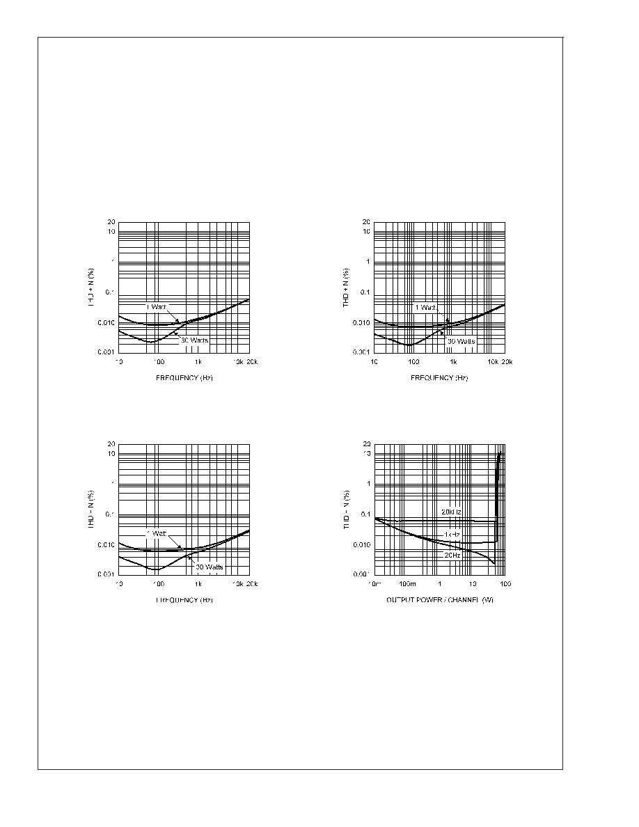
Typical Performance Characteristics
THD+N vs Frequency
±
25V, P
OUT
= 1W & 30W/Channel
R
L
= 4
, 80kHz BW
THD+N vs Frequency
±
30V, P
OUT
= 1W & 30W/Channel
R
L
= 6
, 80kHz BW
200586E3
200586E4
THD+N vs Frequency
±
35V, P
OUT
= 1W & 30W/Channel
R
L
= 8
, 80kHz BW
THD+N vs Output Power/Channel
±
25V, R
L
= 4
, 80kHz BW
200586E5
200586E8
LM4780
www.national.com
9
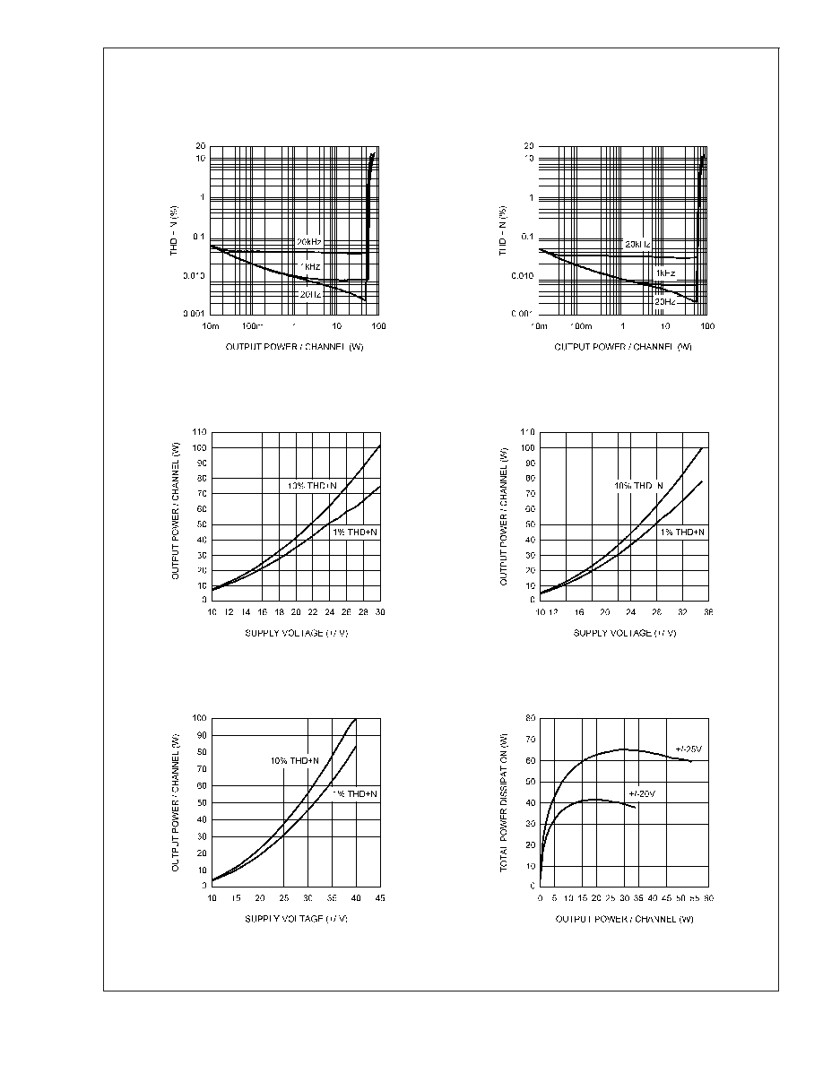
Typical Performance Characteristics
(Continued)
THD+N vs Output Power/Channel
±
30V, R
L
= 6
, 80kHz BW
THD+N vs Output Power/Channel
±
35V, R
L
= 8
, 80kHz BW
200586E9
200586F0
Output Power/Channel
vs Supply Voltage
f = 1kHz, R
L
= 4
, 80kHz BW
Output Power/Channel
vs Supply Voltage
f = 1kHz, R
L
= 6
, 80kHzBW
20058625
20058626
Output Power/Channel
vs Supply Voltage
f = 1kHz, R
L
= 8
, 80kHz BW
Total Power Dissipation
vs Output Power/Channel
1% THD (max), R
L
= 4
, 80kHz BW
20058623
200586A6
LM4780
www.national.com
10
Typical Performance Characteristics
(Continued)
Total Power Dissipation
vs Output Power/Channel
1% THD (max), R
L
= 6
, 80kHz BW
Total Power Dissipation
vs Output Power/Channel
1% THD (max), R
L
= 8
, 80kHz BW
200586A7
200586A8
Crosstalk vs Frequency
±
25V, P
OUT
= 10W
R
L
= 4
, 80kHz BW
Crosstalk vs Frequency
±
35V, P
OUT
= 10W
R
L
= 8
, 80kHz BW
200586C5
200586A5
Mute Attenuation
vs Mute Pin Current
P
OUT
= 10W/Channel
Supply Current
vs Supply Voltage
200586C6
200586B4
LM4780
www.national.com
11
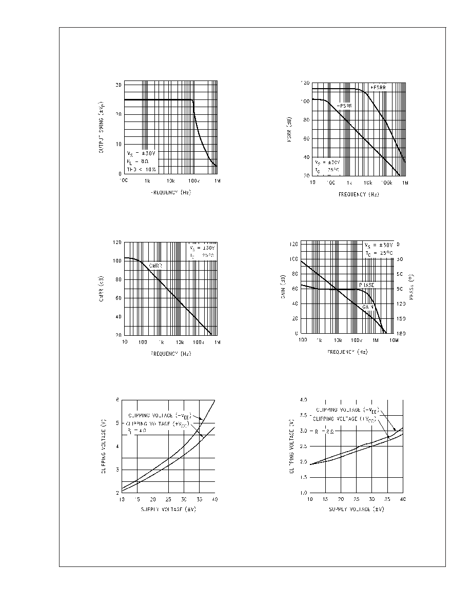
Typical Performance Characteristics
(Continued)
Large Signal Response
Power Supply
Rejection Ratio
200586C7
200586C8
Common Mode
Rejection Ratio
Open Loop
Frequency Response
200586C9
200586D0
Clipping Voltage
vs Supply Voltage
Clipping Voltage
vs Supply Voltage
200586D1
200586D2
LM4780
www.national.com
12
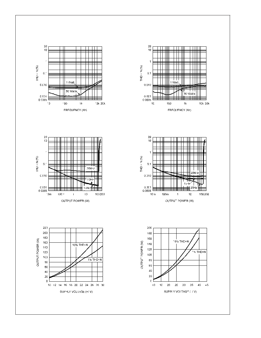
Typical Performance Characteristics
(Continued)
THD+N vs Frequency
±
25V, P
OUT
= 1W & 50W
Bridge Mode (Note 18), R
L
= 8
, 80kHz BW
THD+N vs Frequency
±
35V, P
OUT
= 1W & 50W
Parallel Mode (Note 19), R
L
= 4
, 80kHz BW
200586E6
200586E7
THD+N vs Output Power
±
25V, Bridge Mode (Note 18)
R
L
= 8
, 80kHz BW
THD+N vs Output Power
±
35V, Parallel Mode (Note 19)
R
L
= 4
, 80kHz BW
200586F1
200586F2
Output Power vs
Supply Voltage, Bridge Mode (Note 18)
f = 1kHz, R
L
= 8
, 80kHz BW
Output Power vs
Supply Voltage, Parallel Mode (Note 19)
f = 1kHz, R
L
= 4
, 80kHz BW
20058627
20058624
LM4780
www.national.com
13
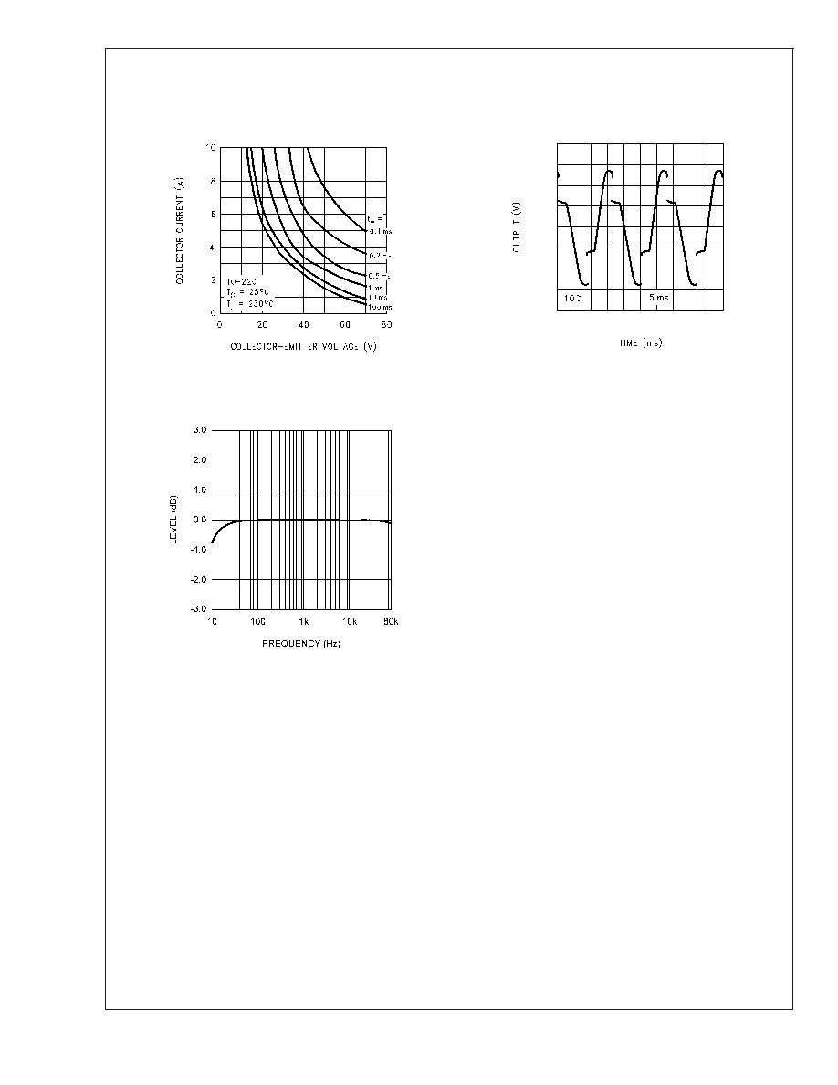
Typical Performance Characteristics
(Continued)
Safe Area
SPiKe
Protection Response
200586D3
200586D4
Frequency Response of Demo Board
P
OUT
= 10W/Channel = 0dB
R
IN
= 47k
, R
L
= 8
, No Filters
200586E2
Note 18: Bridge mode graphs were taken using the demo board and invert-
ing the signal to the channel B input.
Note 19: Parallel mode graphs were taken using the demo board and con-
necting each output through a 0.1
/3W resistor to the load.
LM4780
www.national.com
14
Application Information
MUTE MODE
The muting function allows the user to mute the amplifier.
This can be accomplished as shown in the Typical Applica-
tion Circuit. The resistor R
M
is chosen with reference to the
negative supply voltage and is used in conjunction with a
switch. The switch, when opened or switched to GND, cuts
off the current flow from the MUTE pins to -V
EE
, thus placing
the LM4780 into mute mode. Refer to the Mute Attenuation
vs Mute Current curves in the Typical Performance Char-
acteristics section for values of attenuation per current out
of each MUTE pin. The resistance R
M
is calculated by the
following equation:
R
M
(|-V
EE
| - 2.6V) / I
MUTE
Where I
MUTE
0.5mA for each MUTE pin.
The MUTE pins can be tied together so that only one resistor
is required for the mute function. The mute resistor value
must be chosen so that a minimum of 1mA is pulled through
the resistor R
M
. This ensures that each amplifier is fully
operational. Taking into account supply line fluctuations, it is
a good idea to pull out 1mA per MUTE pin or 2mA total if
both pins are tied together.
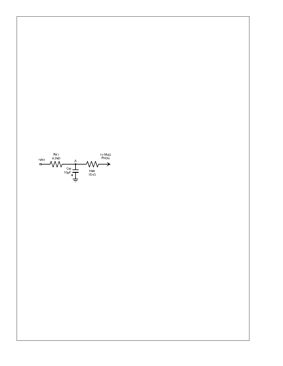
A turn-on MUTE or soft start circuit may also be used during
power up. A simple circuit like the one shown below may be
used.
200586A3
The RC combination of C
M
and R
M1
may cause the voltage
at point A to change more slowly than the -V
EE
supply
voltage. Until the voltage at point A is low enough to have
0.5mA of current per MUTE pin flow through R
M2
, the IC will
be in mute mode. The series combination of R
M1
and R
M2
needs to satisfy the mute equation above for all operating
voltages or mute mode may be activated during normal
operation. For a longer turn-on mute time, a larger time
constant,
= RC = R
M1
C
M
(sec), is needed. For the values
show above and with the MUTE pins tied together, the
LM4780 will enter play mode when the voltage at point A is
-17.6V. The voltage at point A is found with Equation (1)
below.
V
A
(t) = (V
f
- V
O
)e
-t/
(Volts)
(1)
where:
t = time (sec)
= RC (sec)
V
o
= Voltage on C at t = 0 (Volts)
V
f
= Final voltage, -V
EE
in this circuit (Volts)
UNDER-VOLTAGE PROTECTION
Upon system power-up, the under-voltage protection cir-
cuitry allows the power supplies and their corresponding
capacitors to come up close to their full values before turning
on the LM4780. Since the supplies have essentially settled
to their final value, no DC output spikes occur. At power
down, the outputs of the LM4780 are forced to ground before
the power supply voltages fully decay preventing transients
on the output.
OVER-VOLTAGE PROTECTION
The LM4780 contains over-voltage protection circuitry that
limits the output current while also providing voltage clamp-
ing. The clamp does not, however, use internal clamping
diodes. The clamping effect is quite the same because the
output transistors are designed to work alternately by sinking
large current spikes.
SPiKe PROTECTION
The
LM4780
is
protected
from
instantaneous
peak-
temperature stressing of the power transistor array. The Safe
Operating graph in the Typical Performance Characteris-
tics section shows the area of device operation where
SPiKe Protection Circuitry is not enabled. The SPiKe Pro-
tection Response waveform graph shows the waveform dis-
tortion when SPiKe is enabled. Please refer to AN-898 for
more detailed information.
THERMAL PROTECTION
The LM4780 has a sophisticated thermal protection scheme
to prevent long-term thermal stress of the device. When the
temperature on the die exceeds 150∞C, the LM4780 shuts
down. It starts operating again when the die temperature
drops to about 145∞C, but if the temperature again begins to
rise, shutdown will occur again above 150∞C. Therefore, the
device is allowed to heat up to a relatively high temperature
if the fault condition is temporary, but a sustained fault will
cause the device to cycle in a Schmitt Trigger fashion be-
tween the thermal shutdown temperature limits of 150∞C and
145∞C. This greatly reduces the stress imposed on the IC by
thermal cycling, which in turn improves its reliability under
sustained fault conditions.
Since the die temperature is directly dependent upon the
heat sink used, the heat sink should be chosen so that
thermal shutdown is not activated during normal operation.
Using the best heat sink possible within the cost and space
constraints of the system will improve the long-term reliability
of any power semiconductor device, as discussed in the
Determining the Correct Heat Sink section.
DETERMlNlNG MAXIMUM POWER DISSIPATION
Power dissipation within the integrated circuit package is a
very important parameter requiring a thorough understand-
ing if optimum power output is to be obtained. An incorrect
maximum power dissipation calculation may result in inad-
equate heat sinking causing thermal shutdown and thus
limiting the output power.
Equation (2) shows the theoretical maximum power dissipa-
tion point of each amplifier in a single-ended configuration
where V
CC
is the total supply voltage.
P
DMAX
= (V
CC
)
2
/ 2
2
R
L
(2)
Thus by knowing the total supply voltage and rated output
load, the maximum power dissipation point can be calcu-
lated. The package dissipation is twice the number which
results from Equation (2) since there are two amplifiers in
each LM4780. Refer to the graphs of Power Dissipation
versus Output Power in the Typical Performance Charac-
teristics section which show the actual full range of power
dissipation not just the maximum theoretical point that re-
sults from Equation (2).
LM4780
www.national.com
15

Application Information
(Continued)
DETERMINING THE CORRECT HEAT SINK
The choice of a heat sink for a high-power audio amplifier is
made entirely to keep the die temperature at a level such
that the thermal protection circuitry is not activated under
normal circumstances.
The thermal resistance from the die to the outside air,
JA
(junction to ambient), is a combination of three thermal re-
sistances,
JC
(junction to case),
CS
(case to sink), and
SA
(sink to ambient). The thermal resistance,
JC
(junction to
case), of the LM4780T is 0.8∞C/W. Using Thermalloy Ther-
macote thermal compound, the thermal resistance,
CS
(case to sink), is about 0.2∞C/W. Since convection heat flow
(power dissipation) is analogous to current flow, thermal
resistance is analogous to electrical resistance, and tem-
perature drops are analogous to voltage drops, the power
dissipation out of the LM4780 is equal to the following:
P
DMAX
= (T
JMAX
-T
AMB
) /
JA
(3)
where T
JMAX
= 150∞C, T
AMB
is the system ambient tempera-
ture and
JA
=
JC
+
CS
+
SA
.
20058652
Once the maximum package power dissipation has been
calculated using Equation (2), the maximum thermal resis-
tance,
SA
, (heat sink to ambient) in ∞C/W for a heat sink can
be calculated. This calculation is made using Equation (4)
which is derived by solving for
SA
in Equation (3).
SA
= [(T
JMAX
-T
AMB
)-P
DMAX
(
JC
+
CS
)] / P
DMAX
(4)
Again it must be noted that the value of
SA
is dependent
upon the system designer's amplifier requirements. If the
ambient temperature that the audio amplifier is to be working
under is higher than 25∞C, then the thermal resistance for the
heat sink, given all other things are equal, will need to be
smaller.
SUPPLY BYPASSING
The LM4780 has excellent power supply rejection and does
not require a regulated supply. However, to improve system
performance as well as eliminate possible oscillations, the
LM4780 should have its supply leads bypassed with low-
inductance capacitors having short leads that are located
close to the package terminals. Inadequate power supply
bypassing will manifest itself by a low frequency oscillation
known as "motorboating" or by high frequency instabilities.
These instabilities can be eliminated through multiple by-
passing utilizing a large tantalum or electrolytic capacitor
(10µF or larger) which is used to absorb low frequency
variations and a small ceramic capacitor (0.1µF) to prevent
any high frequency feedback through the power supply lines.
If adequate bypassing is not provided, the current in the
supply leads which is a rectified component of the load
current may be fed back into internal circuitry. This signal
causes distortion at high frequencies requiring that the sup-
plies be bypassed at the package terminals with an electro-
lytic capacitor of 470µF or more.
BRIDGED AMPLIFIER APPLICATION
The LM4780 has two operational amplifiers internally, allow-
ing for a few different amplifier configurations. One of these
configurations is referred to as "bridged mode" and involves
driving the load differentially through the LM4780's outputs.
This configuration is shown in Figure 2. Bridged mode op-
eration is different from the classical single-ended amplifier
configuration where one side of its load is connected to
ground.
A bridge amplifier design has a distinct advantage over the
single-ended configuration, as it provides differential drive to
the load, thus doubling output swing for a specified supply
voltage. Theoretically, four times the output power is pos-
sible as compared to a single-ended amplifier under the
same conditions. This increase in attainable output power
assumes that the amplifier is not current limited or clipped.
A direct consequence of the increased power delivered to
the load by a bridge amplifier is an increase in internal power
dissipation. For each operational amplifier in a bridge con-
figuration, the internal power dissipation will increase by a
factor of two over the single ended dissipation. Thus, for an
audio power amplifier such as the LM4780, which has two
operational amplifiers in one package, the package dissipa-
tion will increase by a factor of four. To calculate the
LM4780's maximum power dissipation point for a bridged
load, multiply Equation (2) by a factor of four.
This value of P
DMAX
can be used to calculate the correct size
heat sink for a bridged amplifier application. Since the inter-
nal dissipation for a given power supply and load is in-
creased by using bridged-mode, the heatsink's
SA
will have
to decrease accordingly as shown by Equation (4). Refer to
the section, Determining the Correct Heat Sink, for a more
detailed discussion of proper heat sinking for a given appli-
cation.
PARALLEL AMPLIFIER APPLICATION
Parallel configuration is normally used when higher output
current is needed for driving lower impedance loads (i.e. 4
or lower) to obtain higher output power levels. As shown in
Figure 3 , the parallel amplifier configuration consist of de-
signing the amplifiers in the IC to have identical gain, con-
necting the inputs in parallel and then connecting the outputs
in parallel through a small external output resistor. Any num-
ber of amplifiers can be connected in parallel to obtain the
needed output current or to divide the power dissipation
across multiple IC packages. Ideally, each amplifier shares
the output current equally. Due to slight differences in gain
the current sharing will not be equal among all channels. If
current is not shared equally among all channels then the
power dissipation will also not be equal among all channels.
It is recommended that 0.1% tolerance resistors be used to
set the gain (R
i
and R
f
) for a minimal amount of difference in
current sharing.
When operating two or more amplifiers in parallel mode the
impedance seen by each amplifier is equal to the total load
impedance multiplied by the number of amplifiers driving the
load in parallel as shown by Equation (5) below:
R
L(parallel)
= R
L(total)
* Number of amplifiers
(5)
Once the impedance seen by each amplifier in the parallel
configuration is known then Equation (2) can be used with
this calculated impedance to find the amount of power dis-
sipation for each amplifier. Total power dissipation (P
DMAX
)
within an IC package is found by adding up the power
dissipation for each amplifier in the IC package. Using the
calculated P
DMAX
the correct heat sink size can be deter-
LM4780
www.national.com
16

Application Information
(Continued)
mined. Refer to the section, Determining the Correct Heat
Sink, for more information and detailed discussion of proper
heat sinking.
SINGLE-SUPPLY AMPLIFIER APPLICATION
The typical application of the LM4780 is a split supply am-
plifier. But as shown in Figure 4, the LM4780 can also be
used in a single power supply configuration. This involves
using some external components to create a half-supply bias
which is used as the reference for the inputs and outputs.
Thus, the signal will swing around half-supply much like it
swings around ground in a split-supply application. Along
with proper circuit biasing, a few other considerations must
be accounted for to take advantage of all of the LM4780
functions, like the mute function.
CLICKS AND POPS
In the typical application of the LM4780 as a split-supply
audio power amplifier, the IC exhibits excellent "click" and
"pop" performance when utilizing the mute mode. In addition,
the device employs Under-Voltage Protection, which elimi-
nates unwanted power-up and power-down transients. The
basis for these functions are a stable and constant half-
supply potential. In a split-supply application, ground is the
stable half-supply potential. But in a single-supply applica-
tion, the half-supply needs to charge up at the same rate as
the supply rail, V
CC
. This makes the task of attaining a
clickless and popless turn-on more challenging. Any uneven
charging of the amplifier inputs will result in output clicks and
pops due to the differential input topology of the LM4780.
To achieve a transient free power-up and power-down, the
voltage seen at the input terminals should be ideally the
same. Such a signal will be common-mode in nature, and
will be rejected by the LM4780. In Figure 4, the resistor R
INP
serves to keep the inputs at the same potential by limiting the
voltage difference possible between the two nodes. This
should significantly reduce any type of turn-on pop, due to an
uneven charging of the amplifier inputs. This charging is
based on a specific application loading and thus, the system
designer may need to adjust these values for optimal perfor-
mance.
As shown in Figure 4, the resistors labeled R
BI
help bias up
the LM4780 off the half-supply node at the emitter of the
2N3904. But due to the input and output coupling capacitors
in the circuit, along with the negative feedback, there are two
different values of R
BI
, namely 10k
and 200k. These
resistors bring up the inputs at the same rate resulting in a
popless turn-on. Adjusting these resistors values slightly
may reduce pops resulting from power supplies that ramp
extremely quick or exhibit overshoot during system turn-on.
PROPER SELECTION OF EXTERNAL COMPONENTS
Proper selection of external components is required to meet
the design targets of an application. The choice of external
component values that will affect gain and low frequency
response are discussed below.
The gain of each amplifier is set by resistors R
f
and R
i
for the
non-inverting configuration shown in Figure 1. The gain is
found by Equation (6) below:
A
V
= 1 + R
f
/ R
i
(V/V)
(6)
For best noise performance, lower values of resistors are
used. A value of 1k
is commonly used for R
i
and then
setting the value of R
f
for the desired gain. For the LM4780
the gain should be set no lower than 10V/V and no higher
than 50V/V. Gain settings below 10V/V may experience
instability and using the LM4780 for gains higher than 50V/V
will see an increase in noise and THD.
The combination of R
i
with C
i
(see Figure 1) creates a high
pass filter. The low frequency response is determined by
these two components. The -3dB point can be found from
Equation (7) shown below:
f
i
= 1 / (2
R
i
C
i
) (Hz)
(7)
If an input coupling capacitor is used to block DC from the
inputs as shown in Figure 5, there will be another high pass
filter created with the combination of C
IN
and R
IN
. When
using a input coupling capacitor R
IN
is needed to set the DC
bias point on the amplifier's input terminal. The resulting
-3dB frequency response due to the combination of C
IN
and
R
IN
can be found from Equation (8) shown below:
f
IN
= 1 / (2
R
IN
C
IN
) (Hz)
(8)
With large values of R
IN
oscillations may be observed on the
outputs when the inputs are left floating. Decreasing the
value of R
IN
or not letting the inputs float will remove the
oscillations. If the value of R
IN
is decreased then the value of
C
IN
will need to increase in order to maintain the same -3dB
frequency response.
HIGH PERFORMANCE CONSIDERATIONS
Using low cost electrolytic capacitors in the signal path such
as C
IN
and C
i
(see Figures 1 - 5) will result in very good
performance. However, electrolytic capacitors are less linear
than other premium capacitors. Higher THD+N performance
may be obtained by using high quality polypropylene capaci-
tors in the signal path. A more cost effective solution may be
the use of smaller value premium capacitors in parallel with
the larger electrolytic capacitors. This will maintain signal
quality in the upper audio band where any degradation is
most noticeable while also coupling in the signals in the
lower audio band for good bass response.
Distortion is introduced as the audio signal approaches the
lower -3dB point, determined as discussed in the section
above. By using larger values of capacitors such that the
-3dB point is well outside of the audio band will reduce this
distortion and improve THD+N performance.
Increasing the value of the large supply bypass capacitors
will improve burst power output. The larger the supply by-
pass capacitors the higher the output pulse current without
supply droop increasing the peak output power. This will also
increase the headroom of the amplifier and reduce THD.
SIGNAL-TO-NOISE RATIO
In the measurement of the signal-to-noise ratio, misinterpre-
tations of the numbers actually measured are common. One
amplifier may sound much quieter than another, but due to
improper testing techniques, they appear equal in measure-
ments. This is often the case when comparing integrated
circuit designs to discrete amplifier designs. Discrete transis-
tor amps often "run out of gain" at high frequencies and
therefore have small bandwidths to noise as indicated below.
LM4780
www.national.com
17
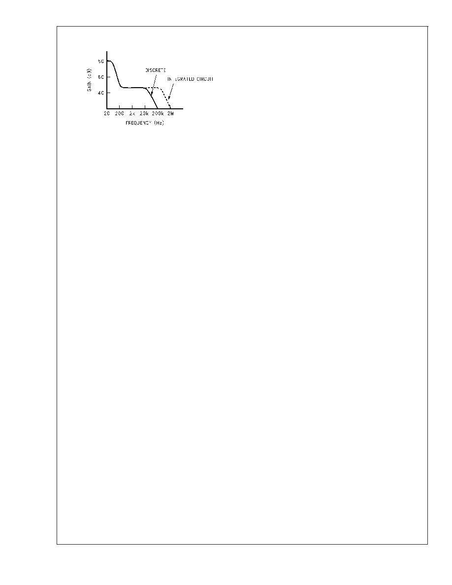
Application Information
(Continued)
20058699
Integrated circuits have additional open loop gain allowing
additional feedback loop gain in order to lower harmonic
distortion and improve frequency response. It is this addi-
tional bandwidth that can lead to erroneous signal-to-noise
measurements if not considered during the measurement
process. In the typical example above, the difference in
bandwidth appears small on a log scale but the factor of 10in
bandwidth, (200kHz to 2MHz) can result in a 10dB theoreti-
cal difference in the signal-to-noise ratio (white noise is
proportional to the square root of the bandwidth in a system).
In comparing audio amplifiers it is necessary to measure the
magnitude of noise in the audible bandwidth by using a
"weighting" filter (Note 16). A "weighting" filter alters the
frequency response in order to compensate for the average
human ear's sensitivity to the frequency spectra. The weight-
ing filters at the same time provide the bandwidth limiting as
discussed in the previous paragraph.
In addition to noise filtering, differing meter types give differ-
ent noise readings. Meter responses include:
1.
RMS reading,
2.
average responding,
3.
peak reading, and
4.
quasi peak reading.
Although theoretical noise analysis is derived using true
RMS based calculations, most actual measurements are
taken with ARM (Average Responding Meter) test equip-
ment.
Typical signal-to-noise figures are listed for an A-weighted
filter which is commonly used in the measurement of noise.
The shape of all weighting filters is similar, with the peak of
the curve usually occurring in the 3kHz≠7kHz region.
LEAD INDUCTANCE
Power op amps are sensitive to inductance in the output
leads, particularly with heavy capacitive loading. Feedback
to the input should be taken directly from the output terminal,
minimizing common inductance with the load.
Lead inductance can also cause voltage surges on the sup-
plies. With long leads to the power supply, energy is stored in
the lead inductance when the output is shorted. This energy
can be dumped back into the supply bypass capacitors when
the short is removed. The magnitude of this transient is
reduced by increasing the size of the bypass capacitor near
the IC. With at least a 20µF local bypass, these voltage
surges are important only if the lead length exceeds a couple
feet (
>
1µH lead inductance). Twisting together the supply
and ground leads minimizes the effect.
PHYSICAL IC MOUNTING CONSIDERATIONS
Mounting of the package to a heat sink must be done such
that there is sufficient pressure from the mounting screws to
insure good contact with the heat sink for efficient heat flow.
Over tightening the mounting screws will cause the package
to warp reducing contact area with the heat sink. Less
contact with the heat sink will increase the thermal resis-
tance from the package case to the heat sink (
CS
) resulting
in higher operating die temperatures and possible unwanted
thermal shut down activation. Extreme over tightening of the
mounting screws will cause severe physical stress resulting
in cracked die and catastrophic IC failure. The recom-
mended mounting screw size is M3 with a maximum torque
of 50 N-cm. Additionally, it is best to use washers under the
screws to distribute the force over a wider area or a screw
with a wide flat head. To further distribute the mounting force
a solid mounting bar in front of the package and secured in
place with the two mounting screws may be used. Other
mounting options include a spring clip. If the package is
secured with pressure on the front of the package the maxi-
mum pressure on the molded plastic should not exceed
150N/mm
2
.
Additionally, if the mounting screws are used to force the
package into correct alignment with the heat sink, package
stress will be increased. This increase in package stress will
result in reduced contact area with the heat sink increasing
die operating temperature and possible catastrophic IC fail-
ure.
LAYOUT, GROUND LOOPS AND STABILITY
The LM4780 is designed to be stable when operated at a
closed-loop gain of 10 or greater, but as with any other
high-current amplifier, the LM4780 can be made to oscillate
under certain conditions. These oscillations usually involve
printed circuit board layout or output/input coupling issues.
When designing a layout, it is important to return the load
ground, the output compensation ground, and the low level
(feedback and input) grounds to the circuit board common
ground point through separate paths. Otherwise, large cur-
rents flowing along a ground conductor will generate volt-
ages on the conductor which can effectively act as signals at
the input, resulting in high frequency oscillation or excessive
distortion. It is advisable to keep the output compensation
components and the 0.1µF supply decoupling capacitors as
close as possible to the LM4780 to reduce the effects of PCB
trace resistance and inductance. For the same reason, the
ground return paths should be as short as possible.
In general, with fast, high-current circuitry, all sorts of prob-
lems can arise from improper grounding which again can be
avoided by returning all grounds separately to a common
point. Without isolating the ground signals and returning the
grounds to a common point, ground loops may occur.
"Ground Loop" is the term used to describe situations occur-
ring in ground systems where a difference in potential exists
between two ground points. Ideally a ground is a ground, but
unfortunately, in order for this to be true, ground conductors
with zero resistance are necessary. Since real world ground
leads possess finite resistance, currents running through
them will cause finite voltage drops to exist. If two ground
return lines tie into the same path at different points there will
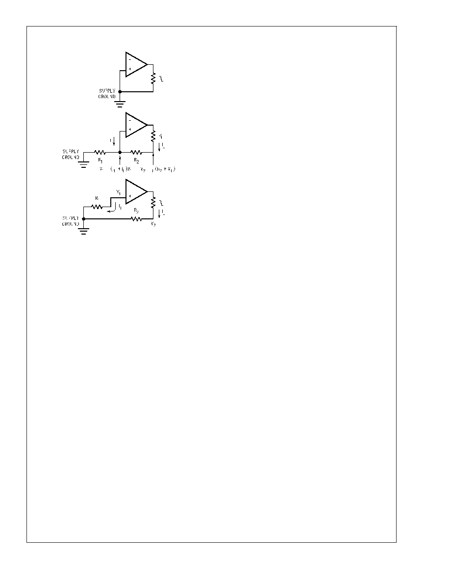
be a voltage drop between them. The first figure below
shows a common ground example where the positive input
ground and the load ground are returned to the supply
ground point via the same wire. The addition of the finite wire
resistance, R
2
, results in a voltage difference between the
two points as shown below.
LM4780
www.national.com
18
Application Information
(Continued)
20058698
The load current I
L
will be much larger than input bias current
I
I
, thus V
1
will follow the output voltage directly, i.e. in phase.
Therefore the voltage appearing at the non-inverting input is
effectively positive feedback and the circuit may oscillate. If
there was only one device to worry about then the values of
R
1
and R
2
would probably be small enough to be ignored;
however, several devices normally comprise a total system.
Any ground return of a separate device, whose output is in
phase, can feedback in a similar manner and cause insta-
bilities. Out of phase ground loops also are troublesome,
causing unexpected gain and phase errors.
The solution to most ground loop problems is to always use
a single-point ground system, although this is sometimes
impractical. The third figure above is an example of a single-
point ground system.
The single-point ground concept should be applied rigor-
ously to all components and all circuits when possible. Vio-
lations of single-point grounding are most common among
printed circuit board designs, since the circuit is surrounded
by large ground areas which invite the temptation to run a
device to the closest ground spot. As a final rule, make all
ground returns low resistance and low inductance by using
large wire and wide traces.
Occasionally, current in the output leads (which function as
antennas) can be coupled through the air to the amplifier
input, resulting in high-frequency oscillation. This normally
happens when the source impedance is high or the input
leads are long. The problem can be eliminated by placing a
small capacitor, C
C
, (on the order of 50pF to 500pF) across
the LM4780 input terminals. Refer to the External Compo-
nents Description section relating to component interaction
with C
f
.
REACTIVE LOADING
It is hard for most power amplifiers to drive highly capacitive
loads very effectively and normally results in oscillations or
ringing on the square wave response. If the output of the
LM4780 is connected directly to a capacitor with no series
resistance, the square wave response will exhibit ringing if
the capacitance is greater than about 0.2µF. If highly capaci-
tive loads are expected due to long speaker cables, a
method commonly employed to protect amplifiers from low
impedances at high frequencies is to couple to the load
through a 10
resistor in parallel with a 0.7µH inductor. The
inductor-resistor combination as shown in the Figure 5 iso-
lates the feedback amplifier from the load by providing high
output impedance at high frequencies thus allowing the 10
resistor to decouple the capacitive load and reduce the Q of
the series resonant circuit. The LR combination also pro-
vides low output impedance at low frequencies thus shorting
out the 10
resistor and allowing the amplifier to drive the
series RC load (large capacitive load due to long speaker
cables) directly.
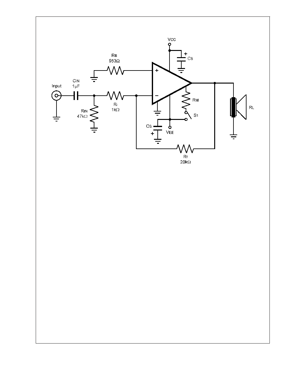
INVERTING AMPLIFIER APPLICATION
The inverting amplifier configuration may be used instead of
the more common non-inverting amplifier configuration
shown in Figure 1. The inverting amplifier can have better
THD+N performance and eliminates the need for a large
capacitor (Ci) reducing cost and space requirements. The
values show in Figure 6 are only one example of an amplifier
with a gain of 20V/V (Gain = -R
f
/R
i
). For different resistor
values, the value of R
B
should be eqaul to the parallel
combination of R
f
and Ri.
If the DC blocking input capacitor (C
IN
) is used as shown, the
lower -3dB point is found using Equation (8) as discussed in
the Proper Selection of External Components section.
LM4780
www.national.com
19
Application Information
(Continued)
20058621
FIGURE 6. Inverting Amplifier Application Circuit
LM4780
www.national.com
20
Application Information
(Continued)
200586F3
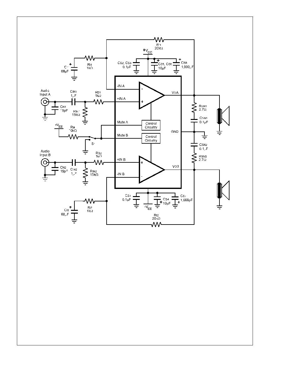
FIGURE 7. Reference PCB Schematic
LM4780
www.national.com
21
Application Information
(Continued)
LM4780 REFERENCE BOARD ARTWORK
200586D9
Composite Layer
200586D8
Silk Layer
200586D7
Top Layer
200586E0
Bottom Layer
LM4780
www.national.com
22
Application Information
(Continued)
BILL OF MATERIALS FOR REFERENCE PCB
Symbol
Value
Tolerance
Type/Description
Comment
R
IN1
, R
IN2
15k
5%
1/4 Watt
R
B1
, R
B2
1k
1%
1/4 Watt
R
F1
, R
F2
20k
1%
1/4 Watt
R
i1
, R
i2
1k
1%
1/4 Watt
R
SN1
, R
SN2
,
2.7
5%
1/4 Watt
R
G
2.7
5%
1/4 Watt
R
M
10k
5%
1/4 Watt
C
IN1
, C
IN2
1µF
10%
Metallized Polyester Film
C
i1
, C
i2
,
68µF
20%
Electrolytic Radial / 50V
C
SN1
, C
SN2
0.1µF
20%
Monolithic Ceramic
C
N1
, C
N2
15pF
20%
Monolithic Ceramic
C
S1
, C
S2
, C
S3
0.1µF
20%
Monolithic Ceramic
C
S4
, C
S5
, C
S6
10µF
20%
Electrolytic Radial / 50V
C
S7
, C
S8
1,000µF
20%
Electrolytic Radial / 50V
S
1
SPDT (on-on) Switch
J
1
, J
2
Non-Switched PC Mount RCA
Jack
J
4
, J
7
, J
8
PCB Banana Jack - BLACK
J
3
, J
5
, J
6
, J
9
PCB Banana Jack - RED
U
1
27 lead TO-220 Power Socket
with push lever release or
LM4780 IC
LM4780
www.national.com
23

Physical Dimensions
inches (millimeters)
unless otherwise noted
Non-Isolated TO-220 27-Lead Package
Order Number LM4780TA
NS Package Number TA27A
LIFE SUPPORT POLICY
NATIONAL'S PRODUCTS ARE NOT AUTHORIZED FOR USE AS CRITICAL COMPONENTS IN LIFE SUPPORT
DEVICES OR SYSTEMS WITHOUT THE EXPRESS WRITTEN APPROVAL OF THE PRESIDENT AND GENERAL
COUNSEL OF NATIONAL SEMICONDUCTOR CORPORATION. As used herein:
1. Life support devices or systems are devices or
systems which, (a) are intended for surgical implant
into the body, or (b) support or sustain life, and
whose failure to perform when properly used in
accordance with instructions for use provided in the
labeling, can be reasonably expected to result in a
significant injury to the user.
2. A critical component is any component of a life
support device or system whose failure to perform
can be reasonably expected to cause the failure of
the life support device or system, or to affect its
safety or effectiveness.
National Semiconductor
Americas Customer
Support Center
Email: new.feedback@nsc.com
Tel: 1-800-272-9959
National Semiconductor
Europe Customer Support Center
Fax: +49 (0) 180-530 85 86
Email: europe.support@nsc.com
Deutsch Tel: +49 (0) 69 9508 6208
English
Tel: +44 (0) 870 24 0 2171
FranÁais Tel: +33 (0) 1 41 91 8790
National Semiconductor
Asia Pacific Customer
Support Center
Email: ap.support@nsc.com
National Semiconductor
Japan Customer Support Center
Fax: 81-3-5639-7507
Email: jpn.feedback@nsc.com
Tel: 81-3-5639-7560
www.national.com
LM4780
Overture
TM
Audio
Power
Amplifier
Series
Stereo
60W
,
Mono
120W
Audio
Power
Amplifier
with
Mute
National does not assume any responsibility for use of any circuitry described, no circuit patent licenses are implied and National reserves the right at any time without notice to change said circuitry and specifications.