LM4804
Low Voltage High Power Audio Power Amplifier
General Description
The LM4804 integrates a Boost Converter with an Audio
Power Amplifier to drive voice coil speakers in portable
applications. When powered by a 3V supply, it is capable of
creating 1.8W power dissipation in an 8
bridge-tied-load
(BTL) with less than 1% THD+N.
Boomer audio power amplifiers were designed specifically to
provide high quality output power with a minimal amount of
external components. The LM4804 does not require boot-
strap capacitors, or snubber circuits. Therefore it is ideally
suited for portable applications requiring high output voltage
and minimal size.
The LM4804 features a micro-power shutdown mode. Addi-
tionally, the LM4804 features an internal thermal shutdown
protection mechanism.
The LM4804 contains advanced pop & click circuitry that
eliminates output transients which would otherwise occur
during power or shutdown cycles.
The LM4804 is unity-gain stable. Its closed-loop gain is
determined by the value of external, user selected resistors.
Key Specifications
j
Quiescent Power Supply Current
(V
DD
= 4.2V, R
L
= 8
)
11mA (typ)
j
BTL Output Power
(R
L
= 8
, 2% THD+N, V
DD
= 3V)
1.8W (typ)
j
Shutdown Current
2µA (max)
Features
n
Pop & click circuitry eliminates noise during turn-on and
turn-off transitions
n
Low, 2µA (max) shutdown current
n
Low, 11mA (typ) quiescent current (V
DD
= 4.2V, R
L
=
8
)
n
1.8W mono BTL output, R
L
= 8
, V
DD
= 3V
n
Short circuit protection
n
Unity-gain stable
n
External gain configuration capability
Applications
n
Cellphone
n
PDA
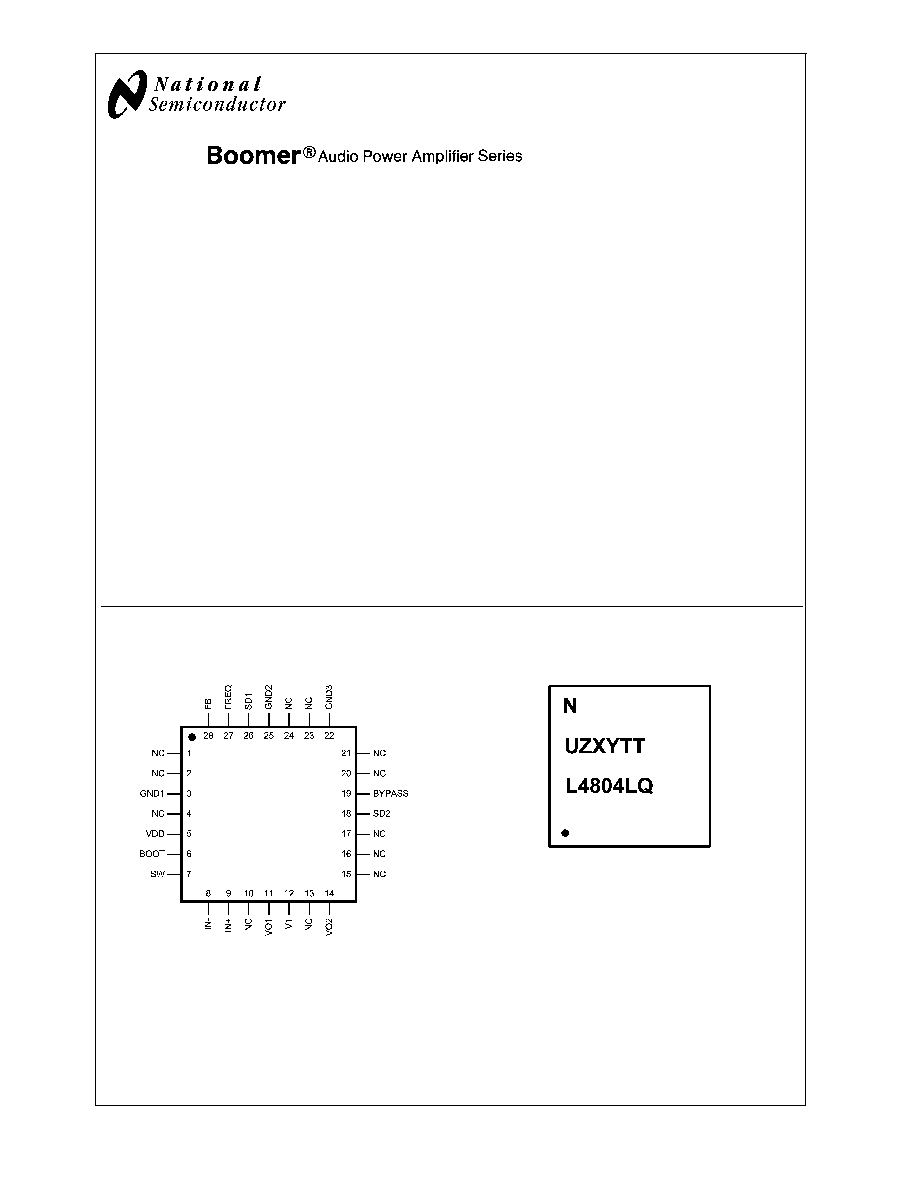
Connection Diagrams
LM4804LQ (5x5)
LQ Marking
20116784
Top View
Order Number LM4804LQ
See NS Package Number LQA28A
20116737
Top View
U = Wafer Fab Code
Z = Assembly Plant Code
XY = Date Code
TT = Die Run Code
Boomer
®
is a registered trademark of National Semiconductor Corporation.
March 2005
LM4804
Low
V
oltage
High
Power
Audio
Power
Amplifier
© 2005 National Semiconductor Corporation
DS201167
www.national.com
Absolute Maximum Ratings
(Notes 1, 2)
If Military/Aerospace specified devices are required,
please contact the National Semiconductor Sales Office/
Distributors for availability and specifications.
Supply Voltage (V
DD
)
6.5V
Supply Voltage (V
1
)
6.5V
Storage Temperature
-65°C to +150°C
Input Voltage
-0.3V to V
DD
+ 0.3V
Power Dissipation (Note 3)
Internally limited
ESD Susceptibility (Note 4)
2000V
ESD Susceptibility (Note 5)
200V
Junction Temperature
125°C
Thermal Resistance
JA
(LLP)
59°C/W
See AN-1187 'Leadless Leadframe Packaging (LLP).'
Operating Ratings
Temperature Range
T
MIN
T
A
T
MAX
-40°C
T
A
+85°C
Supply Voltage (V
DD
)
3V
V
DD
5V
Supply Voltage (V
1
)
2.7V
V
1
6.1V
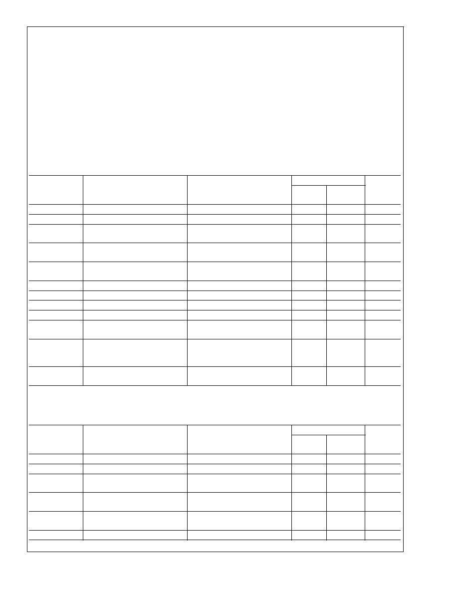
Electrical Characteristics V
DD
= 4.2V
(Notes 1, 2)
The following specifications apply for V
DD
= 4.2V, V
1
= 6.0V, A
V-BTL
= 20dB, R
L
= 8
, f
IN
= 1kHz, C
B
= 1.0µF, R
1
= 301k
, R
2
= 78.7k
unless otherwise specified. Limits apply for T
A
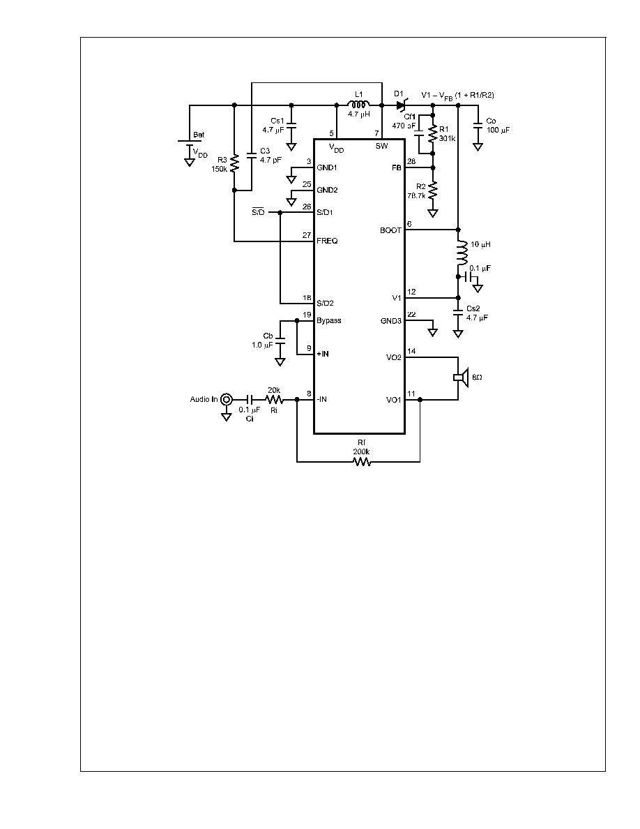
= 25°C. See Figure 1.
Symbol
Parameter
Conditions
LM4804
Units
(Limits)
Typical
(Note 6)
Limit
(Notes 7, 8)
I
DD
Quiescent Power Supply Current
V
IN
= 0, R
LOAD
=
11
22
mA (max)
I
SD
Shutdown Current
V
SHUTDOWN
= GND (Notes 9, 10)
0.1
2
µA (max)
V
SDIH
Shutdown Voltage Input High
SD1
SD2
0.7V
DD
1.4
V (min)
V
SDIL
Shutdown Voltage Input Low
SD1
SD2
0.15V
DD
0.4
V (max)
T
WU
Wake-up Time
C
B
= 1.0µF
70
msec
(max)
V
OS
Output Offset Voltage
4
40
mV (max)
TSD
Thermal Shutdown Temperature
125
°C (min)
P
OUT
Output Power
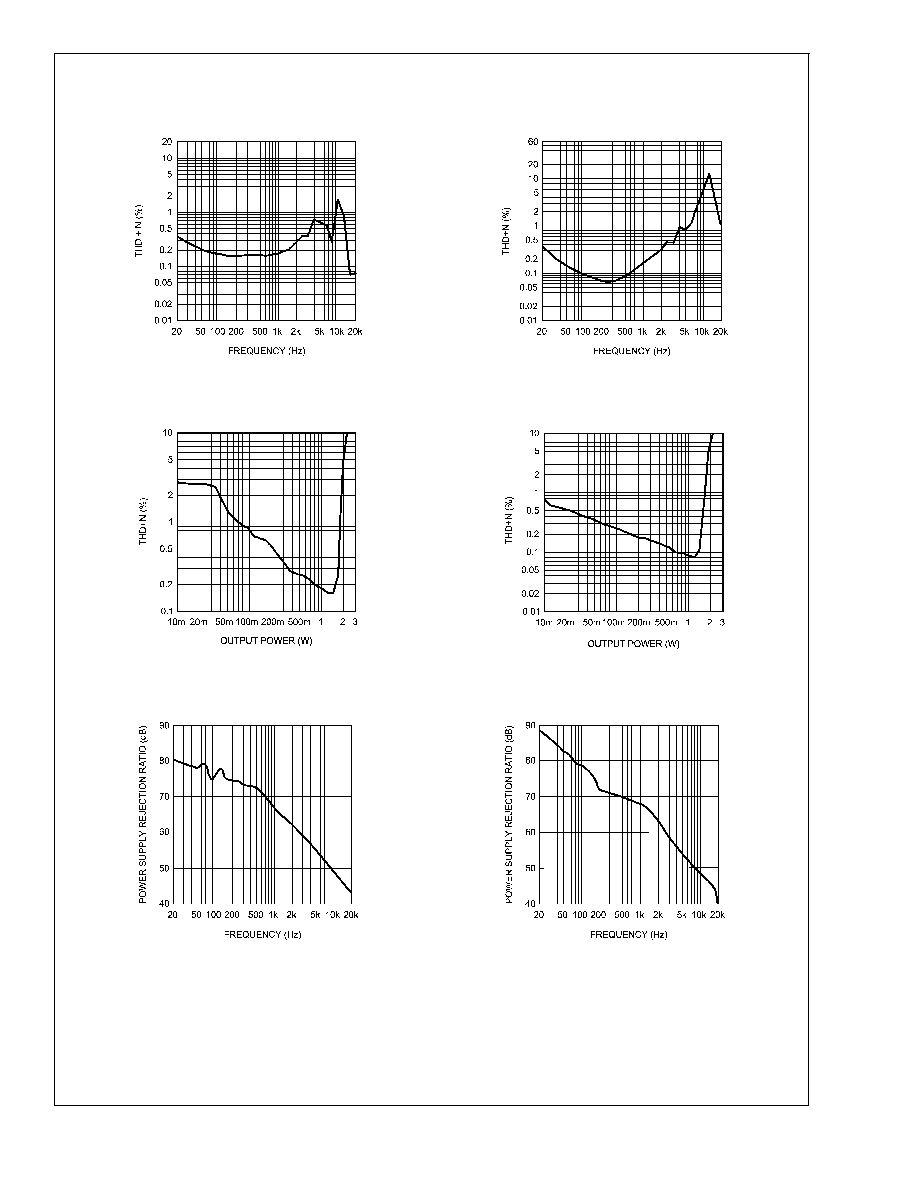
THD = 2% (max)
1.9
1.7
W (min)
THD+N
Total Harmomic Distortion + Noise
P
OUT
= 1.5W
0.13
0.5
%
e
OS
Output Noise
A-Weighted Filter, V
IN
= 0V,
Input Referred
22
µV
PSRR
Power Supply Rejection Ratio
V
RIPPLE
= 200mV
p-p
f = 217Hz
f = 1kHz
72
67
dB (min)
V
FB
Feedback Pin Reference Voltage
1.24
1.2772
1.2028
V (max)
V (min)
Electrical Characteristics V
DD
= 3.0V
(Notes 1, 2)
The following specifications apply for V
DD
= 3.0V, V
1
= 6.0V, A
V-BTL
= 20dB, R
L
= 8
, f
IN
= 1kHz, C
B
= 1.0µF, R
1
= 301k
, R
2
= 78.7k
unless otherwise specified. Limits apply for T
A
= 25°C.
Symbol
Parameter
Conditions
LM4804
Units
(Limits)
Typical
(Note 6)
Limit
(Notes 7, 8)
I
DD
Quiescent Power Supply Current
V
DD
= 3.2V, V
IN
= 0, R
LOAD
=
19
33
mA (max)
I
SD
Shutdown Current
V
SHUTDOWN
= GND (Notes 9, 10)
0.1
2
µA (max)
V
SDIH
Shutdown Voltage Input High
SD1
SD2
0.7V
DD
1.4
V (min)
V
SDIL
Shutdown Voltage Input Low
SD1
SD2
0.15V
DD
0.4
V (max)
T
WU
Wake-up Time
C
B
= 1.0µF
70
msec
(max)
V
OS
Output Offset Voltage
3
40
mV (max)
LM4804
www.national.com
3
Electrical Characteristics V
DD
= 3.0V
(Notes 1, 2) (Continued)
The following specifications apply for V
DD
= 3.0V, V
1
= 6.0V, A
V-BTL
= 20dB, R
L
= 8
, f
IN
= 1kHz, C
B
= 1.0µF, R
1
= 301k
, R
2
= 78.7k
unless otherwise specified. Limits apply for T
A
= 25°C.
Symbol
Parameter
Conditions
LM4804
Units
(Limits)
Typical
(Note 6)
Limit
(Notes 7, 8)
TSD
Thermal Shutdown Temperature
125
°C (min))
P
OUT
Output Power
THD = 2% (max)
1.8
1.65
W (min)
THD+N
Total Harmomic Distortion + Noise
P
OUT
= 1.5W
0.15
0.5
%
e
OS
Output Noise
A-Weighted Filter, V
IN
= 0V,
Input Referred
30
µV
PSRR
Power Supply Rejection Ratio
V
RIPPLE
= 200mV
p-p
f = 217Hz
f = 1kHz
73
66
dB (min)
V
FB
Feedback Pin Reference Voltage
(Note 11)
1.24
1.2772
1.2028
V (max)
V (min)
Note 1: All voltages are measured with respect to the GND pin, unless otherwise specified.
Note 2: Absolute Maximum Ratings indicate limits beyond which damage to the device may occur. Operating Ratings indicate conditions for which the device is
functional, but do not guarantee specific performance limits. Electrical Characteristics state DC and AC electrical specifications under particular test conditions which
guarantee specific performance limits. This assumes that the device is within the Operating Ratings. Specifications are not guaranteed for parameters where no limit
is given, however, the typical value is a good indication of device performance.
Note 3: The maximum power dissipation must be derated at elevated temperatures and is dictated by T
JMAX
,
JA
, and the ambient temperature, T
A
. The maximum
allowable power dissipation is P
DMAX
= (T
JMAX
- T
A
) /
JA
or the given in Absolute Maximum Ratings, whichever is lower.
Note 4: Human body model, 100pF discharged through a 1.5k
resistor.
Note 5: Machine Model, 220pF 240pF discharged through all pins.
Note 6: Typicals are measured at 25°C and represent the parametric norm.
Note 7: Limits are guaranteed to National's AOQL (Average Outgoing Quality Level).
Note 8: Datasheet min/max specification limits are guaranteed by design, test, or statistical analysis.
Note 9: Shutdown current is measured in a normal room environment. The Shutdown pin should be driven as close as possible to V
in
for minimum shutdown
current.
Note 10: Shutdown current is measured with components R1 and R2 removed.
Note 11: Feedback pin reference voltage is measured with the Audio Amplifier disconnected from the Boost converter (the Boost converter is unloaded).
LM4804
www.national.com
4