 | –≠–ª–µ–∫—Ç—Ä–æ–Ω–Ω—ã–π –∫–æ–º–ø–æ–Ω–µ–Ω—Ç: LM4830 | –°–∫–∞—á–∞—Ç—å:  PDF PDF  ZIP ZIP |

LM4830
Two-Way Audio Amplification System
with Volume Control
General Description
The LM4830 is an integrated solution for two-way audio am-
plification. It contains a bridge-connected audio power ampli-
fier capable of delivering 1W of continuous average power to
an 8
load with less than 1% THD from a 5V power supply.
It also has the capability of driving 100 mW into a
single-ended 32
impedance for headset operation. There
is a 30 dB attenuator in front of a bridged power amplifier
with 6 dB of gain. The attenuation is controlled through 4 bits
of parallel digital control; 15 steps of 2 dB each.
The device also contains a microphone preamp with two se-
lectable inputs. Mic2 is selected when HS is high and A1 is in
single-ended mode. Mic1 is selected when HS is low and A1
is in bridged mode. This configuration is optimum for switch-
ing between an internal system speaker and external head-
set with microphone. The device also incorporates a buffer
used for driving capacitive loads.
The LM4830 also provides a low-current consumption shut-
down mode making it optimally suited for low-power portable
systems. In addition, the device has an internal thermal shut-
down protection mechanism.
Key Specifications
n
THD at 1W cont. avg P
O
into 8
:
1% (max)
n
Instantaneous peak output power:
1.4W
n
Shutdown current:
0.5 µA (typ)
n
Supply voltage range:
2.7V
V
DD
5.5V
Features
n
4-bit digital control for 30 dB of volume attenuation
n
Two selectable microphone inputs
n
High performance microphone preamp
n
Extra buffer for driving long cables
n
No bootstrap capacitors or snubber circuits are
necessary
n
Small Outline (SO) packaging
n
Thermal shutdown protection circuitry
Applications
n
Hands-free phone systems
n
Mobile phone accessories
n
Desktop conference phones
n
Portable computers
n
Teleconference computer applications
Connection Diagram
Dual-In-Line and
Small Outline Packages
DS012677-2
Top View
Order Number LM4830M
See NS Package Number M24B for SO
Order Number LM4830N
See NS Package Number N24A for DIP
January 1999
LM4830
T
wo-W
ay
Audio
Amplification
System
with
V
olume
Control
© 1999 National Semiconductor Corporation
DS012677
www.national.com
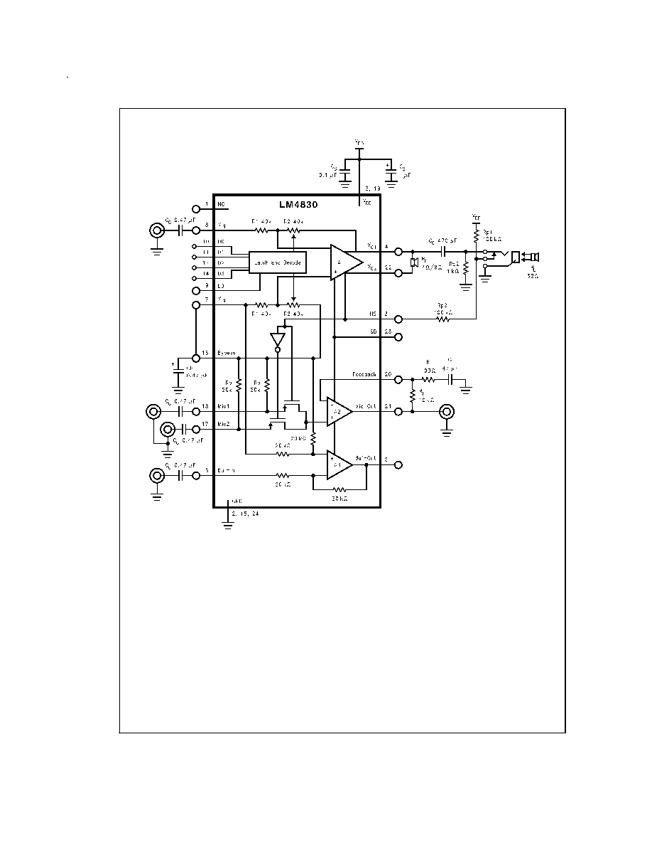
Typical Application
DS012677-1
FIGURE 1. Typical Application Circuit
www.national.com
2
Absolute Maximum Ratings
(Note 2)
If Military/Aerospace specified devices are required,
please contact the National Semiconductor Sales Office/
Distributors for availability and specifications.
Supply Voltage
6.0V
Storage Temperature
-65∞C to +150∞C
Input Voltage
-0.3V to V
DD
+ 0.3V
Power Dissipation (Note 3)
Internally Limited
ESD Susceptibility (Note 4)
2000V
ESD Susceptibility (Note 5)
250V
Junction Temperature
150∞C
Soldering Information
Small Outline Package
Vapor Phase (60 sec.)
215∞C
Infrared (15 sec.)
220∞C
See AN-450
"Surface Mounting and their Effects on
Product Reliability" for other methods of soldering surface
mount devices.
Operating Ratings
Temperature Range
T
MIN
T
A
T
MAX
-40∞C
T
A
85∞C
Supply Voltage
2.7V
V
DD
5.5V
JC
(typ) -- M24B
32∞C/W
JA
(typ) -- M24B
79∞C/W
JC
(typ) -- N24A
21∞C/W
JA
(typ) -- N24A
61∞C/W
Electrical Characteristics
(Notes 1, 2)
The following specifications apply for V
DD
= 5V, unless otherwise specified. Limits apply for T
A
= 25∞C.
Symbol
Parameter
Conditions
LM4830
Units
(Limits)
Typical
Limit
(Note 6)
(Note 7)
POWER AMPLIFIER, A1
I
DD
Quiescent Power Supply Current
V
O
= 0V, I
O
= 0A, R
L
=
5.8
mA (min)
11.0
20.0
mA (max)
Bridged R
L
= 8
11.4
mA
HS = 5V, SD = 0V, V
O1
On Only
7.9
mA
I
SD
Shutdown Current
HS = 5V, SD = 5V, IC Off
0.5
2.0
µA (max)
V
OS
Output Offset Voltage
V
IN
= 0V
0.7
50.0
mV (max)
e
IN
Input Noise
IHF-A Weighting Filter, R
S
= 25
Bridged Output, V
O1
≠V
O2
, R
L
= 8
30
µV
Single-Ended Output, V
O1
, R
L
= 32
16
µV
P
O
Output Power, Bridged
THD = 1% (max); f = 1 kHz, R
L
= 8
1.15
1.0
W (min)
THD+N = 10%; f = 1 kHz, R
L
= 8
1.4
W
THD+N = 10%; f = 1 kHz, R
L
= 4
2
W
THD
Total Harmonic Distortion
f = 1 kHz, Attenuation
@
0 dB
P
O
= 1.5W, R
L
= 4
0.2
%
P
O
= 1W, R
L
= 8
0.2
%
V
O1
On Only, V
O
= 60 mV, R
L
= 32
0.06
%
Attenuation Step Size Error
0 dB to -30 dB
±
0.5
dB
Absolute Attenuation
Attenuation
@
0 dB
±
0.5
dB
Attenuation
@
-30 dB
±
1.0
dB
R
IN
Power Amp Input Resistance
40
k
DIGITAL INPUTS
V
IH
High Input Voltage
CMOS Compatible Only
4.5
V
V
IL
Low Input Voltage
CMOS Compatible Only
0.5
V
PREAMP, A2
R
IN
Mic1 and Mic2 Input Resistance
21.5
k
V
OS
Output Offset Voltage
V
IN
= 0V
2.0
mV
e
IN
Input Noise
IHF-A Weighting Filter, R
S
= 25
1.3
10.0
µV (max)
THD
Total Harmonic Distortion
A
VCL
= 100, V
IN
= 10 mVrms, f = 1 kHz
0.06
%
A
VCL
= -1, P
O
= 50 mW, f = 1 kHz, R
L
=
32
0.02
(Refer to
Figure 2 )
www.national.com
3
Electrical Characteristics
(Notes 1, 2) (Continued)
The following specifications apply for V
DD
= 5V, unless otherwise specified. Limits apply for T
A
= 25∞C.
Symbol
Parameter
Conditions
LM4830
Units
(Limits)
Typical
Limit
(Note 6)
(Note 7)
PREAMP, A2
Xtalk
Crosstalk
A
VCL
= 100, Power Amp: P
O
= 1W,
R
L
= 8
, f = 1 kHz
-72
dB
PSRR
Power Supply Rejection Ratio
V
DDAC
= 0.5 V
PP
, f = 1 kHz
60
dB
MICROPHONE BUFFER, A3
R
IN
Buffer Input Resistance
17
k
V
OS
Output Offset Voltage
V
IN
= 0V
2.0
mV
e
IN
Input Noise
IHF-A Weighting Filter, R
S
= 25
5.8
µV
THD
Total Harmonic Distortion
P
O
= 50 mW, f = 1 kHz, R
L
= 32
0.5
%
Xtalk
Crosstalk
Power Amp: P
O
= 1W, R
L
= 8
, f = 1 kHz
-76
dB
Note 1: All voltages are measured with respect to the ground pins (Pins 2, 15, and 24), unless otherwise specified.
Note 2: Absolute Maximum Ratings indicate limits beyond which damage to the device may occur. Operating Ratings indicate conditions for which the device is func-
tional, but do not guarantee specific performance limits. Electrical Characteristics state DC and AC electrical specifications under particular test conditions which guar-
antee specific performance limits. This assumes that the device is within the Operating Ratings. Specifications are not guaranteed for parameters where no limit is
given, however, the typical value is a good indication of device performance.
Note 3: The maximum power dissipation must be derated at elevated temperatures and is dictated by T
JMAX
,
JA
, and the ambient temperature, T
A
. The maximum
allowable power dissipation is P
DMAX
= (T
JMAX
- T
A
)/
JA
or the number given in the Absolute Maximum Ratings, whichever is lower. For the LM4830M, T
JMAX
=
+150∞C, and the typical junction-to-ambient thermal resistance, when board mounted, is 79∞C/W.
Note 4: Human body model, 100 pF discharged through a 1.5 k
resistor.
Note 5: Machine model, 200 pF≠240 pF discharged through all pins.
Note 6: Typicals are measured at 25∞C and represent the parametric norm.
Note 7: Limits are guarantees that all parts are tested in production to meet the stated values.
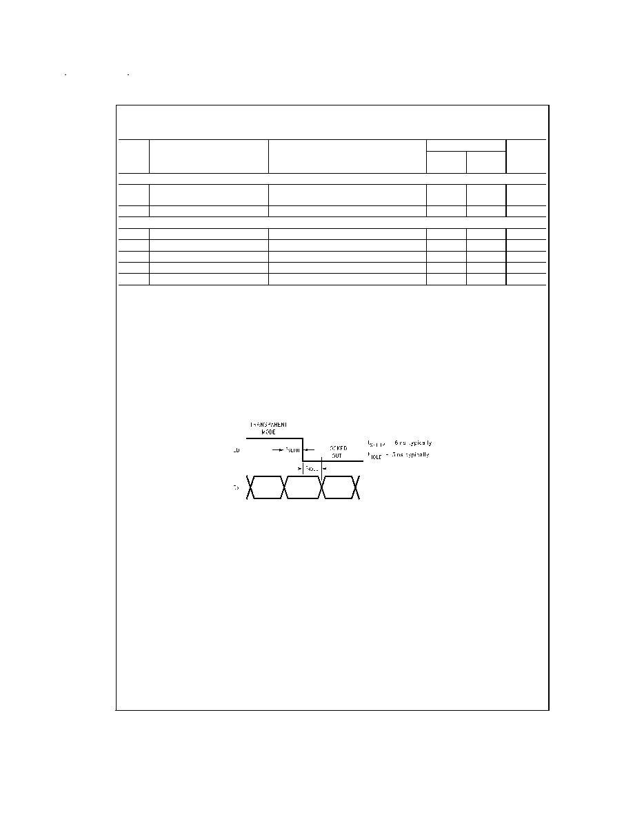
Timing Diagram
DS012677-3
www.national.com
4
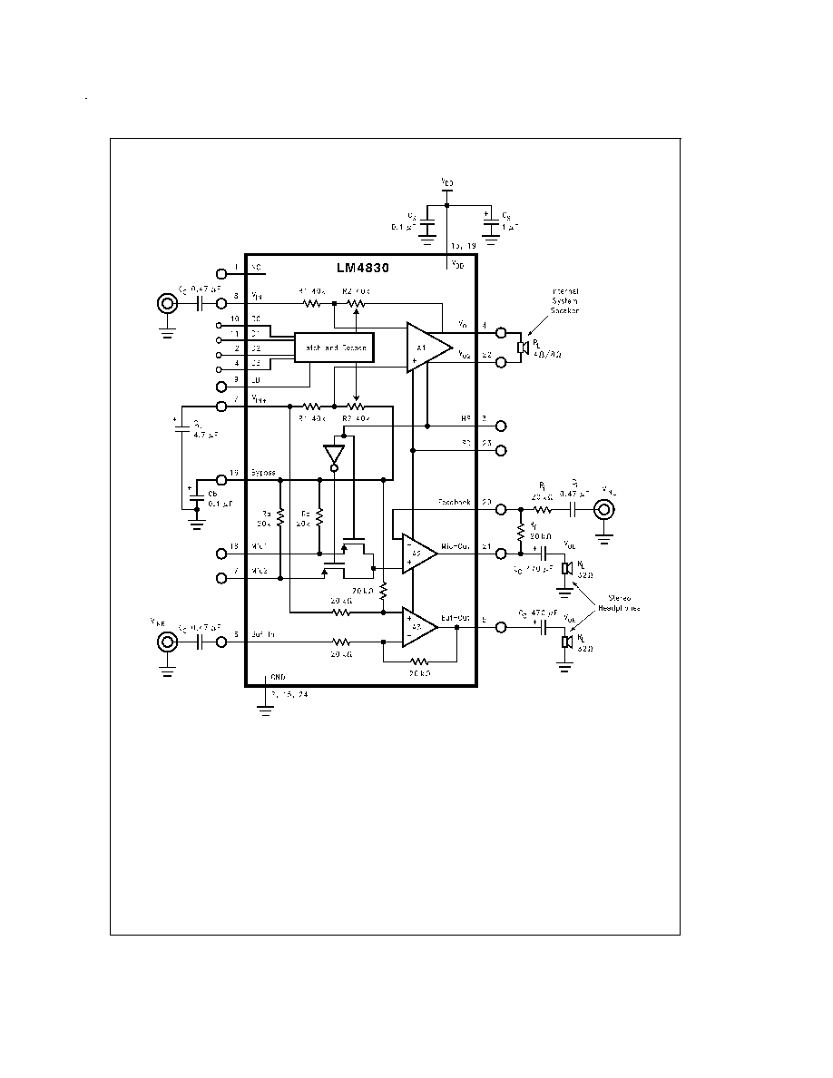
Computer Application Circuit
DS012677-4
FIGURE 2.
www.national.com
5