 | –≠–ª–µ–∫—Ç—Ä–æ–Ω–Ω—ã–π –∫–æ–º–ø–æ–Ω–µ–Ω—Ç: LM4831VF | –°–∫–∞—á–∞—Ç—å:  PDF PDF  ZIP ZIP |
LM4831
Multimedia Computer Audio Chip
General Description
The LM4831 is a monolithic integrated circuit that provides a
stereo three input mixer, two stereo input analog multiplexer,
a stereo line out and a dual 1W bridged audio power ampli-
fier. In addition, a low noise microphone preamp is included
on-chip.
The LM4831 is ideal for multimedia computers since it incor-
porates an input mixer, analog multiplexer, and configurable
stereo audio power amplifier, as well as a microphone
preamp stage. This combination allows for all of the analog
audio processing to be enclosed in a 44-pin TQFP package.
The LM4831 features an externally controlled, low-power
consumption shutdown mode, as well as both headphone
and docking station modes. To temporarily override the shut-
down mode and allow audio signals to be amplified, the
LM4831 provides four "beep" pins.
Key Specifications
n
THD+N at 1W into 8
0.6% (typ)
n
Microphone Input Referred Noise
10µV (typ)
n
Supply Current - Bridged Mode
16mA (typ)
n
Shutdown Current
2µA (typ)
Features
n
Stereo 1W audio power amplifier
n
"Click and pop" suppression circuitry
n
Stereo three input mixer
n
Shutdown mode
n
Multiple operating modes -- bridged, single-ended and
docking station modes
n
Internal mux for switching in/out external filter
n
Beep circuitry for "wake-up" while in shutdown
n
44 Pin TQFP Packaging
Applications
n
Portable and Desktop Computers
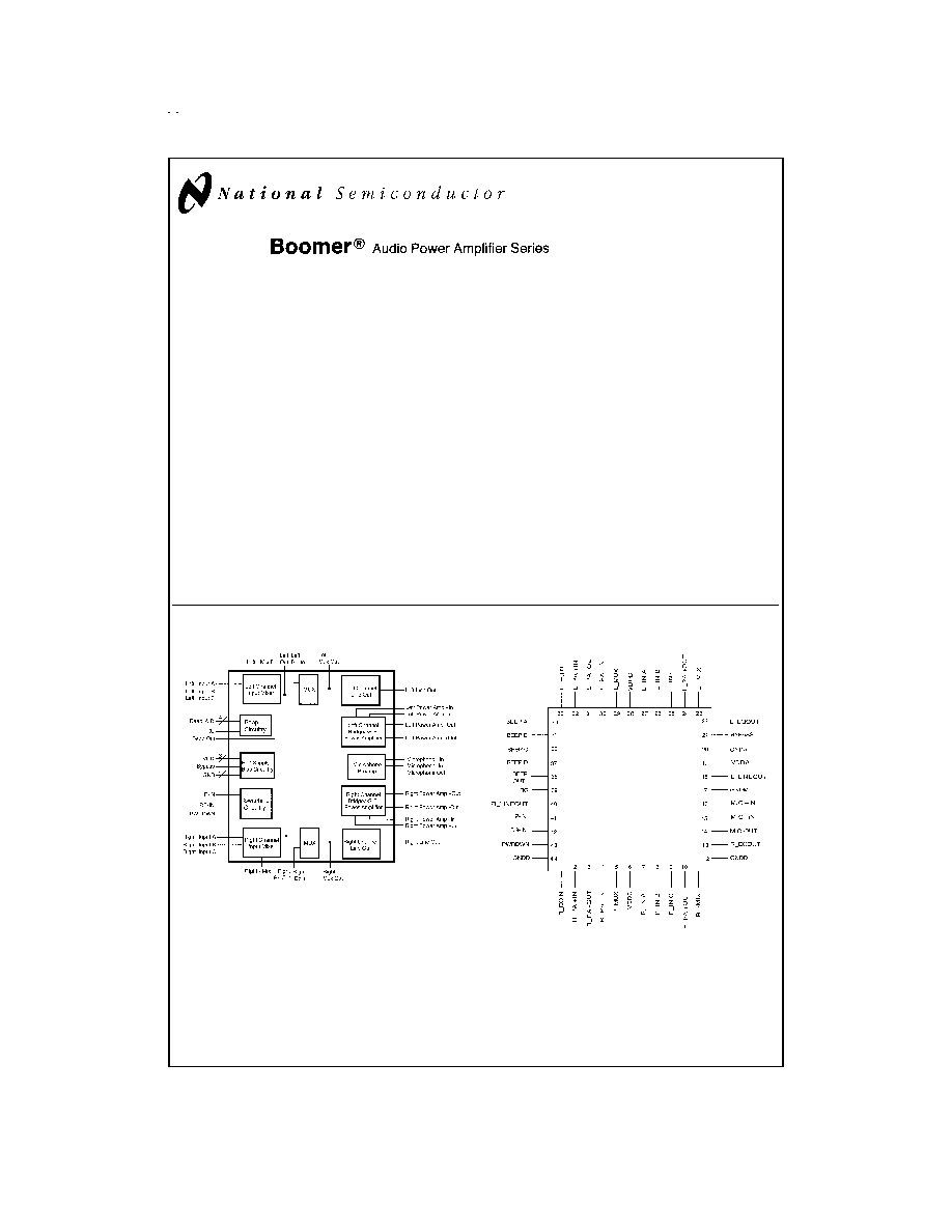
Block Diagram
Connection Diagram
Boomer
Æ
is a registered trademark of National Semiconductor Corporation.
TRI-STATE
Æ
is a registered trademark of National Semiconductor Corporation.
DS100057-1
FIGURE 1. LM4831 Block Diagram
DS100057-3
Top View
Order Number LM4831VF
See NS Package Number VEJ44A
November 1998
LM4831
Multimedia
Computer
Audio
Chip
© 1998 National Semiconductor Corporation
DS100057
www.national.com

Absolute Maximum Ratings
(Note 2)
If Military/Aerospace specified devices are required,
please contact the National Semiconductor Sales Office/
Distributors for availability and specifications.
Supply Voltage
6.0V
Storage Temperature
-65∞C to 150∞C
Input Voltage
-0.3V to V
DD
+0.3V
Power Dissipation (Note 3)
Internally limited
ESD Susceptibility (Note 4)
2500V
ESD Susceptibility (Note 5)
200V
Junction Temperature
150∞C
Soldering Information
Small Outline Package
Vapor Phase (60 sec.)
215∞C
Infrared (15 sec.)
220∞C
See AN-450 "Surface Mounting and their Effects on
Product Reliability" for other methods of soldering
surface mount devices.
Thermal Resistance
JC
(typ)
15∞C/W
JA
(typ)
62∞C/W
Operating Ratings
Temperature Range
-40∞C to 85∞C
Supply Voltage
2.7
V
DD
5.5V
Electrical Characteristics
(Notes 1, 2) The following specifications apply for V
DD
= 5V, R
L
= 8
and f = 1 kHz, unless otherwise specified. Distortion
measurements represent the full audio chain from Input A of each channel to their respective output. Limits apply for
T
A
= 25∞C.
Symbol
Parameter
Conditions
LM4831
Units
(Limits)
Typical
(Note
6)
Limit
(Note
7)
General Characteristics For Entire IC
V
DD
Supply Voltage
2.7
V (min)
5.5
V (max)
I
DD
Quiescent Power Supply
Current
Bridged Mode, I
O
= 0 mA
16
50
mA (max)
Single-Ended Mode, I
O
= 0 mA
10.5
mA
Docking Station Mode, I
O
= 0 mA
7
mA
I
SD
Shutdown Current
V
PIN-43
= 5V, V
PIN-41
= V
PIN-42
= 0V
2
50
µA (max)
V
DD/2
Half Supply Bypass Voltage
V
IN
= 0V, V
Pin-43
= 0V
2.45
2.4
V (min)
2.6
V (max)
Power Amplifiers
P
O
Output Power - Bridged
Mode
R
L
= 8
,THD = 1%
1.1
1
W (min)
R
L
= 4
, THD = 1%
1.5
W
Output Power -
Single-Ended Mode
R
L
= 8
, THD = 1%
300
mW
R
L
= 4
, THD = 1%
550
mW
THD
Total Harmonic Distortion
Bridged Mode, P
O
= 1W, R
L
= 8
0.5
2.0
% (Max)
Single-Ended Mode, P
O
= 225mW,
R
L
= 8
0.15
%
V
OS
Output Offset Voltage
V
IN
= 0V
5
50
mV (Max)
E
Noise
Input Referred Noise
A-Weighted Filter, V
IN
= 0V,
R
L
= 8
Bridged Output
45
100
µV (max)
Single-Ended Output
35
100
µV (max)
PSRR
Power Supply Rejection
Ratio
f = 1kHz, C
B
= 0.5µF, R
L
= 8
Bridged Output
47
dB
Single-Ended Output
45
dB
X
TALK
Channel to Channel
Crosstalk
f = 1kHz, P
O
= 1W, R
L
= 8
Right to Left
-82
dB
Left to Right
-73
dB
I
TS
TRI-STATE
Æ
Current-Single
Ended Mode
V
PIN-41
= 4.0V, L_PA+OUT =
R_PA+OUT = V
DD
or GND
80
100
µA (max)
www.national.com
2
Electrical Characteristics
(Continued)
(Notes 1, 2) The following specifications apply for V
DD
= 5V, R
L
= 8
and f = 1 kHz, unless otherwise specified. Distortion
measurements represent the full audio chain from Input A of each channel to their respective output. Limits apply for
T
A
= 25∞C.
Symbol
Parameter
Conditions
LM4831
Units
(Limits)
Typical
(Note
6)
Limit
(Note
7)
Microphone Amplifier
THD
Total Harmonic Distortion
R
L
= 10 k
, V
IN
= 1 V
RMS
0.15
%
E
Noise
Input Referred Noise
A--weighted Filter
10
18
µV (max)
X
TALK
Crosstalk
Amplifier Bridged Output, f = 1kHz,
P
O
= 1W, R
L-mic
= 20k
95
dB
Other Audio Characteristics
THD
Total Harmonic Distortion
R
L
= 20 k
, V
IN
= 1 V
RMS
Line Out
0.15
0.5
% (max)
Equalizer Out
0.01
%
E
Noise
Input Referred Noise
A-weighted filter, Line Out
20
100
µV (max)
A
V
Channel Path Gain
Line Out
±
0.1
±
0.7
dB (max)
Equalizer Out
±
0.1
±
0.6
dB (max)
MUX Out
-0.25
-0.85,
+0.3
dB
E
T
Stereo Tracking Error
Line Out
±
0.1
±
0.5
dB (max)
Digital Inputs and Outputs
V
IL
Input Low Voltage
1.0
V (max)
V
IH
Input High Voltage
4.0
V (min)
V
OL
Output Low Voltage
0.5
V (max)
V
OH
Output High Voltage
3.5
V (min)
Note 1: All voltages are measured with respect to the ground pins, 12, 17, 20, and 44, unless otherwise specified.
Note 2:
Absolute Maximum Ratings indicate limits beyond which damage to the device may occur. Operating Ratings indicate conditions for which the device is func-
tional, but do not guarantee specific performance limits.
Electrical Characteristics state DC and AC electrical specifications under particular test conditions which guar-
antee specific performance limits. This assumes that the device is within the Operating Ratings. Specifications are not guaranteed for parameters where no limit is
given, however, the typical value is a good indication of device performance.
Note 3: The maximum power dissipation must be derated at elevated temperatures and is dictated by T
JMAX
,
JA
, and the ambient temperature T
A
. The maximum
allowable power dissipation is P
DMAX
= (T
JMAX
- T
A
)/
JA
. For the LM4831, T
JMAX
= 150∞C, and the typical junction-to-ambient thermal resistance, when board
mounted, is 62∞C/W assuming the VEF44A package.
Note 4: Human body model, 100 pF discharged through a 1.5 k
resistor.
Note 5: Machine Model, 220 pF≠240 pF discharged through all pins.
Note 6: Typicals are measured at 25∞C and represent the parametric norm.
Note 7: Limits are guaranteed to National's AOQL (Average Outgoing Quality Level).
Digital Inputs Pin Truth Table
Pin Name
LM4831 State
PWRDWN
HPIN
DSIN
0
0
0
Bridged Outputs Active
Equalizer In/Out Active
0
0
1
Line-Outs Active
0
1
X(Note 8)
Single-Ended Outputs Active
1
X
X
Shutdown
Note 8: "X" means that the state of that pin does not matter in that particular input combination.
www.national.com
3
Typical Application
DS100057-2
FIGURE 3. Typical Application Circuit
www.national.com
4

Pin Descriptions
VDDA
This is the analog power supply pin
which powers all internal circuitry, with
the exceptions of the output amplifiers
and the digital logic in the Beep and
Switching circuit sections. This pin
should be connected to the same
supply voltage as the two VDDD pins
(typically 5V), but have a separate
ground return path to the supply
ground to minimize interaction with the
high current amplifier returns and
digital switching noise. In addition, this
pin should be bypassed with a 0.01
µF≠0.1 µF capacitor.
VDDD
These pins are the "digital" and high
current power supply pins which
power the stereo bridged output
amplifier and the digital logic in the
Beep and Switching circuit sections.
These pins should be connected to
the same supply voltage as the VDDA
pin (typically 5V), but have a separate
return path to the supply to avoid
interferring with low level signals. In
addition, this pin should be bypassed
with a 0.01 µF≠0.1 µF capacitor. At
the power supply connection, a bulk
storage capacitor of at least 10 µF will
reduce the instantaneous current
demanded from the power supply.
GNDA,
GNDD,
GNDM
These are the power supply ground
pins. GNDA is the ground pin for the
low current analog circuitry. The two
GNDD pins are for the digital logic
and bridged output amplifiers. GNDM
is the ground for the microphone
amplifier. Make sure that the high
current GNDD paths are not returned
through the low current GNDM or
GNDA paths. These four ground pins
should be star-grounded at a stable,
low-impedance, noise-free system
ground.
BYPASS
This voltage at this pin is nominally
1/2 VDDD and is created by an
internal 50 k
resistor divider. This
node should be bypassed with a
capacitor value from 0.1 µF-1.0 µF.
Increasing the capacitor value will
increase the ramp time of the
amplifiers, thereby improving turn-on
pop performance. 0.1µF is typical for
the bypass capacitor. In addition, a 1
M
resistor from the bypass pin to the
positive supply is shown in Figure 3.
This resistor guarantees that the
LM4831 will turn-on if the device is
powered up with both the PWRDWN
and DS-IN pins high. If the the
LM4831 will never enter that state,
then the 1M
resistor can be
removed.
HP-IN
This pin places the output power
amplifier in "headphone" mode. If
HP-IN is low, the amplifier is in
bridged mode and the 2:1 mux passes
the input on the EQ_IN pin. If HP-IN is
high, the amplifier is in single-ended
mode and the 2:1 mux passes the
output of the mixing stage.
Single-ended mode places the
non-inverting amplifier in the output
amplifiers into a high impedance state.
HP-IN also has priority over the DS-IN
pin, so if HP-IN and DS-IN are both
high, the device is in single-ended
mode and the stereo line out amplifier
is in a high-impedance state.
DS-IN
This pin is used to put the LM4831
into "docking-station" mode and
control the line out drivers and the
state of the internal 2:1 analog
multiplexer. If DS-IN is high, the
stereo line out amplifier is on and the
stereo bridged amplifier is in a high
impedance state. Asserting the DS-IN
pin also changes the 2:1 analog
multiplexer output from the stereo
signal on the L_EQIN and R_EQIN
pins to the internal path from the
stereo input mixer.
www.national.com
5