 | –≠–ª–µ–∫—Ç—Ä–æ–Ω–Ω—ã–π –∫–æ–º–ø–æ–Ω–µ–Ω—Ç: LM4832 | –°–∫–∞—á–∞—Ç—å:  PDF PDF  ZIP ZIP |
LM4832
Digitally Controlled Tone and Volume Circuit with Stereo
Audio Power Amplifier, Microphone Preamp Stage and
National 3D Sound
General Description
The LM4832 is a monolithic integrated circuit that provides
volume and tone (bass and treble) controls as well as a ste-
reo audio power amplifier capable of producing 250 mW
(typ) into 8
or 90 mW (typ) into 32
with less than 1.0%
THD. In addition, a two input microphone preamp stage, with
volume control, capable of driving a 1 k
load is imple-
mented on chip.
The LM4832 also features National's 3D Sound circuitry
which can be externally adjusted via a simple RC network.
For maximum system flexibility, the LM4832 has an exter-
nally controlled, low-power consumption shutdown mode,
and an independent mute for power and microphone ampli-
fiers .
Boomer
Æ
audio integrated circuits were designed specifically
to provide high quality audio while requiring few external
components. Since the LM4832 incorporates tone and vol-
ume controls, a stereo audio power amplifier and a micro-
phone preamp stage, it is optimally suited to multimedia
monitors and desktop computer applications.
Key Specifications
n
Output Power at 10% into:
8
32
350 mW(typ)
100 mW(typ)
n
THD + N at 75 mW into
32
at 1 kHz
0.5%(max)
n
Microphone Input Referred
Noise
7 µV(typ)
n
Supply Current
13 mA(typ)
n
Shutdown Current
4 µA(max)
Features
n
Independent Left and Right Output Volume Controls
n
Treble and Bass Control
n
National 3D Sound
n
I
2
C Compatible Interface
n
Two Microphone Inputs with Selector
n
Software Controlled Shutdown Function
Applications
n
Multimedia Monitors
n
Portable and Desktop Computers
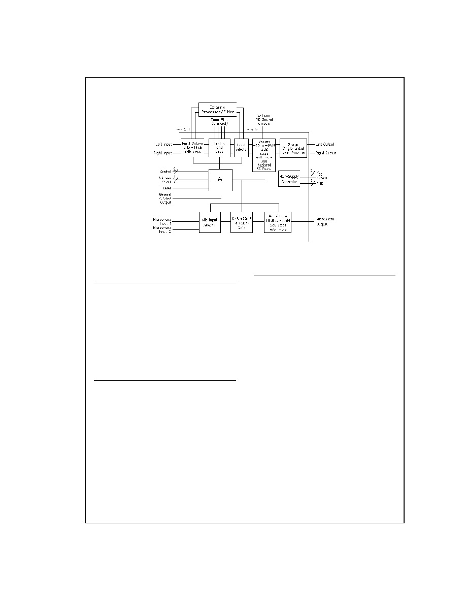
Block Diagram
Connection Diagram
Boomer
Æ
is a registered trademark of National Semiconductor Corporation.
DS100014-1
FIGURE 1. LM4832 Block Diagram
DS100014-2
Top View
Order Number LM4832N, LM4832M
See NS Package Number N28B for DIP
See NS Package Number M28B for SOIC
February 1998
LM4832
Digitally
Controlled
T
one
and
V
olume
Circuit
with
Stereo
Audio
Power
Amplifier
,
Microphone
Preamp
Stage
and
National
3D
Sound
© 1998 National Semiconductor Corporation
DS100014
www.national.com

Absolute Maximum Ratings
(Note 2)
If Military/Aerospace specified devices are required,
please contact the National Semiconductor Sales Office/
Distributors for availability and specifications.
Supply Voltage
6.0V
Storage Temperature
-65∞C to +150∞C
Input Voltage
-0.3V to V
DD
+0.3V
Power Dissipation (Note 3)
Internally limited
ESD Susceptibility (Note 4)
2000V
ESD Susceptibility (Note 5)
250V
Junction Temperature
150∞C
Soldering Information
Small Outline Package
Vapor Phase (60 sec.)
215∞C
Infrared (15 sec.)
220∞C
See AN-450
Surface Mounting and their Effects on
Product Reliability
for other methods of soldering
surface mount devices.
JC
(typ)--N28B
21∞C/W
JA
(typ)--N28B
62∞C/W
JC
(typ)--M28B
15∞C/W
JA
(typ)--M28B
69∞C/W
Operating Ratings
Temperature Range
T
MIN
T
A
T
MAX
-40∞C
T
A
85∞C
Supply Voltage
4.5
V
DD
5.5V
Electrical Characteristics for Entire IC
(Notes 1, 2)
The following specifications apply for V
DD
= 5V unless otherwise noted. Limits apply for T
A
= 25∞C.
Symbol
Parameter
Conditions
LM4832
Units
(Limits)
Typical
(Note 6)
Limit
(Note 7)
V
DD
Supply Voltage
V
IN
= 0V, I
O
= 0A
4.5
V (min)
5.5
V (max)
I
DD
Quiescent Power Supply Current
13
21
mA (max)
I
SD
Shutdown Current
2.5
9
µA (max)
INPUT ATTENUATORS
A
R
Attenuator Range
Attenuation at 0 dB Setting
Attenuation at -14 dB Setting
1
-15
dB (max)
dB (min)
A
S
Step Size
0 dB to -14 dB
2
dB
Gain Step Size Error
0.1
dB (max)
E
T
Channel to Channel Tracking Error
0.15
dB (max)
BASS CONTROL
A
R
Bass Control Range
f = 100 Hz, V
IN
= 0.25V
±
12
-14
dB (min)
14
dB (max)
A
S
Bass Step Size
2
dB
E
SE
Bass Step Size Error
0.5
dB (max)
E
T
Bass Tracking Error
0.15
dB (max)
TREBLE CONTROL
A
R
Treble Control Range
f
IN
= 10 kHz, V
IN
= 0.25V
±
12
-13
dB (min)
13
dB (max)
A
S
Treble Step Size
2
dB
E
SE
Treble Step Size Error
0.1
dB (max)
E
T
Treble Tracking Error
0.15
dB (max)
OUTPUT ATTENUATORS
A
R
Attenuator Range
Gain at +20 dB Setting
Attenuation at -40 dB Setting
+20 dB to -40 dB
21
dB (max)
-42
dB (min)
A
S
Step Size
2
dB
Step Size Error
0.1
dB (max)
E
T
Channel to Channel Tracking Error
0.1
dB (max)
AUDIO PATH
V
OS
Output Offset Voltage
V
IN
= 0V
3
50
mV (max)
www.national.com
2
Electrical Characteristics for Entire IC
(Notes 1, 2) (Continued)
The following specifications apply for V
DD
= 5V unless otherwise noted. Limits apply for T
A
= 25∞C.
Symbol
Parameter
Conditions
LM4832
Units
(Limits)
Typical
(Note 6)
Limit
(Note 7)
AUDIO PATH
P
O
Output Power
THD = 1.0% (max), f = 1 kHz, All
controls at 0dB
R
L
= 8
250
mW (min)
R
L
= 32
95
75
mW (min)
THD+N
Total Harmonic Distortion+Noise
All Controls at 0 dB, THD = 10%, f = 1
kHz
R
L
= 8
350
mW
P
O
= 200 mW, R
L
= 8
0.15
%
P
O
= 75 mW, R
L
= 32
0.11
%
V
O
= 1 Vrms, R
L
= 10
0.08
%
PSRR
Power Supply Rejection Ratio
C
B
= 1 µF, f = 100 Hz, V
RIPPLE
= 100
mVrms, All Controls at 0 dB Setting
45
dB
A
M
Mute Attenuation
f = 1 kHz, V
IN
= 1V
-75
dB
X
TALK
Cross Talk
P
O
= 200 mW, R
L
= 8
,
All controls at 0 dB setting,
f = 1 kHz
Left to Right
-85
dB
Right to Left
-72
dB
MICROPHONE PREAMP AND VOLUME CONTROL
A
V
Preamp Gain
0 dB Gain
0
-1, 1
dB
+20 dB Gain
20
19, 21
dB
+30 dB Gain
30
29, 31
dB
A
R
Attenuator Range
Gain at +18 dB Setting
20
dB (max)
Attenuation at -42 dB Setting
-43
dB (min)
A
S
Step Size
0 dB to -42 dB
3
dB
Step Size Error
0.4
dB (max)
V
SWING
Output Voltage Swing
f = 1 kHz, THD
<
1.0%, R
L
= 1 k
1.7
V
rms
E
NO
Input Referred Noise
A-Weighted, Attenuator at 0 dB
7
µV (min)
PSRR
Power Supply Rejection Ratio
f = 100 Hz, V
RIPPLE
= 100 mVrms,
C
B
= 1 µF
35
dB
A
M
Mute Attenuation
-90
dB
X
TALK
Cross Talk
Power Amp P
O
= 200 mW, f = 1 kHz
-90
dB
THD+N
Total Harmonic Distortion Plus Noise
All controls at 0 dB, f = 1 kHz, V
O
= 1V
0 dB Setting
0.03
%
+20 dB Gain
0.03
%
+30 dB Gain
0.04
%
I
2
C BUS TIMING
f
MAX
Maximum Bus Frequency
400
kHz
T
START:HOLD
Start Signal: Hold Time before
Clock/Data Transitions
0.6
µs
T
D;SETUP
Data Setup Time
0.1
µs
T
C;HIGH
Minimum High Clock Duration
0.6
µs
T
C;LOW
Minimum Low Clock Duration
1.3
µs
T
STOP;SETUP
Stop Signal: Setup Time before
Clock/Data Transitions
0.6
µs
I
2
C BUS INPUT AND OUTPUT
V
IL
Input Low Voltage
1.5
V (max)
3
www.national.com

Electrical Characteristics for Entire IC
(Notes 1, 2) (Continued)
The following specifications apply for V
DD
= 5V unless otherwise noted. Limits apply for T
A
= 25∞C.
Symbol
Parameter
Conditions
LM4832
Units
(Limits)
Typical
(Note 6)
Limit
(Note 7)
I
2
C BUS INPUT AND OUTPUT
V
IH
Input High Voltage
3
V (min)
I
IN
Input Current
0.15
µA
V
O
Output Voltage--SDA Acknowledge
0.4
V (max)
V
OL
External Power Amp Disable Low
0.4
V (max)
V
OH
External Power Amp Disable High
4
V (min)
Note 1: All voltages are measured with respect to the ground pins, unless otherwise specified. All specifications are tested using the typical applicationas shown in
Figure 1.
Note 2: Absolute Maximum Ratings indicate limits beyond which damage to the device may occur. Operating Ratings indicate conditions for which the device is func-
tional, but do not guarantee specific performance limits. Electrical Characteristics state DC and AC electrical specifications under particular test conditions which guar-
antee specific performance limits. This assumes that the device is within the Operating Ratings. Specifications are not guaranteed for parameters where no limit is
given, however, the typical value is a good indication of device performance.
Note 3: The maximum power dissipation must be derated at elevated temperatures and is dictated by T
JMAX
,
JA
, and the ambient temperature T
A
. The maximum
allowable power dissipation is P
DMAX
= (T
JMAX
- T
A
)/
JA
.For the LM4832, T
JMAX
= 150∞C, and the typical junction-to-ambient thermal resistance, when board
mounted, is 69∞C/W assuming the M28B package.
Note 4: Human body model, 100 pF discharged through a 1.5 k
resistor.
Note 5: Machine Model, 220 pF≠240 pF discharged through all pins.
Note 6: Typicals are measured at 25∞C and represent the parametric norm.
Note 7: Limits are guaranteed that all parts are tested in production to meet the stated values.
Typical Application Circuit
DS100014-3
FIGURE 2. Typical Application Circuit
www.national.com
4

Pin Description
LEFT 3D (1)
RIGHT 3D
(28)
An external RC network is connected
across these pins. This function provides
left-right channel cross coupling and
cancellation to create an enhanced
stereo channel separation effect.
BYPASS (2)
A 0.1 µF capacitor is placed between
this pin and ground to provide an AC
ground for the internal half-supply
voltage reference. The capacitor at this
pin affects "click-pop" and THD
performance. Turn-on and turn-off times
are also determined by this capacitor.
Refer to the Application Information
section for more information.
POWER
AMP OUT
LEFT (3)
RIGHT (26)
These outputs are intended to drive 8
speakers or 32
headphones. These
outputs should be AC-coupled to the
loads. Refer to the Application
Information section for more information.
POWER
GND (4)
This pin provides the high current return
for the power output stage MOSFETs
and digital circuitry.
LOOP OUT
(8, 21)
LOOP IN (5,
24)
These pins allow an external signal
processor access to the stereo signal.
Please see the Application Information
section for more information.
TONE OUT
(6, 23)
These pins are connected to the tone
control op amp outputs and drive the
power amplifier inputs. Refer to the
Application Information section for more
information.
TONE IN
(7, 22)
These pins are connected to the inputs
of the tone control op amps. A capacitor
between the Tone In and Tone Out pins
sets the frequency response of the tone
functions. Please refer to the Application
Information section for more information.
INPUTS
(9, 20)
These pins are the stereo inputs for the
LM4832. These pins should be
AC-coupled to the input signals.
ANALOG
GND (10)
This pin is the AC analog ground for the
line level AC signal inputs.
MIC
INPUTS
(11, 12)
These pins are the two independent
selectable microphone inputs. These
pins should be AC-coupled.
MIC OUT
(14)
This pin is the output for the microphone
amplifier and should be AC-coupled to
the load.
V
DD
(13, 25)
These pins are for the 5V supply. These
pins should be separately bypassed by
0.1 µF, or higher, film capacitors. The 5V
supply should be bypassed by a 10 µF,
or higher, tantalum or aluminum
electrolytic capacitor.
ADDRESS
BITS (15,
16)
These pins are used to determine the
I
2
C address for the LM4832.
CLOCK (17)
This pin is the input for the I
2
C clock
signal.
DATA (18)
This pin is the input for the I
2
C data
signal.
GENERAL
PURPOSE
OUTPUT
(19)
This pin provides a general purpose
TTL/CMOS output. Please refer to the
Application Information section for more
information.
RESET (27)
This pin is a TTL/CMOS input which is
used to reset the chip logic and states.
5
www.national.com
Typical Performance Characteristics
THD+N vs
Frequency, 8
DS100014-4
THD+N vs
Frequency, 32
DS100014-5
THD+N vs
Frequency, 1 k
DS100014-6
THD+N vs
Output Power
DS100014-7
THD+N vs
Output Power
DS100014-8
THD+N vs
Output Power
DS100014-9
Power Amplifier
Crosstalk
DS100014-10
Power Amplifier
Noise Floor
DS100014-11
Power Amplifier Attenuation
vs Frequency
DS100014-12
www.national.com
6
Typical Performance Characteristics
(Continued)
Power Supply
Rejection Ratio
DS100014-13
Power Dissipation
vs Output Power
DS100014-14
Power Derating
Curve
DS100014-15
Mic Amplifer Crosstalk
from Power Amplifier
DS100014-16
Mic Amplifier
Noise Floor
DS100014-17
Mic Amplifier Attenuation
vs Frequency
DS100014-18
Mic Amplifier Gain
vs Frequency
DS100014-19
Mic Amplifier THD+N
vs Frequency
DS100014-20
Loop-out THD+N
vs Frequency
DS100014-21
7
www.national.com
Typical Performance Characteristics
(Continued)
Timing Diagram
Bass Response
vs Frequency
DS100014-22
Treble Response
vs Frequency
DS100014-23
Bass and Treble Response
vs Frequency
DS100014-24
Supply Current
vs Temperature
DS100014-25
DS100014-26
FIGURE 3. I
2
C Bus Format
www.national.com
8
Timing Diagram
(Continued)
DS100014-27
See Electrical Characteristics section fortiming specifications
FIGURE 4. I
2
C Timing Diagram
9
www.national.com
Truth Tables
SOFTWARE SPECIFICATION
Chip Address
MSB
LSB
1
0
0
0
0
*E.C.
*E.C.
0
*E.C. = Externally Configuarable
Data Bytes (Brief Description)
MSB
LSB
Function
0
0
0
X
X
D2
D1
D0
Input Volume Control
0
0
1
X
D3
D2
D1
D0
Bass Control
0
1
0
X
D3
D2
D1
D0
Treble Control
0
1
1
D4
D3
D2
D1
D0
Right Output Vol./Mute
1
0
0
D4
D3
D2
D1
D0
Left Output Vol./Mute
1
0
1
X
D
1
1
D
1
0
D
0
1
D
0
0
Mic Input and Gain
1
1
0
D4
D3
D2
D1
D0
Microphone Volume
1
1
1
D
4
0
D
3
0
D
2
0
D
1
0
D
0
0
General Control
Input Volume Control
MSB
LSB
Attenuation (dB)
0
0
0
X
X
0
0
0
0
0
0
0
X
X
0
0
1
-2
0
0
0
X
X
0
1
0
-4
0
0
0
X
X
0
1
1
-6
0
0
0
X
X
1
0
0
-8
0
0
0
X
X
1
0
1
-10
0
0
0
X
X
1
1
0
-12
0
0
0
X
X
1
1
1
-14
Input Volume Control
Power Up State
X
X
0
0
0
Input Volume Control
at 0 dB Attenuation
Bass Control
MSB
LSB
Level (dB)
0
0
1
X
0
0
0
0
-12
0
0
1
X
0
0
0
1
-10
0
0
1
X
0
0
1
0
-8
0
0
1
X
0
0
1
1
-6
0
0
1
X
0
1
0
0
-4
0
0
1
X
0
1
0
1
-2
0
0
1
X
0
1
1
0
0
0
0
1
X
0
1
1
1
2
0
0
1
X
1
0
0
0
4
0
0
1
X
1
0
0
1
6
0
0
1
X
1
0
1
0
8
0
0
1
X
1
0
1
1
10
0
0
1
X
1
1
0
0
12
Bass Control
Power Up State
X
0
1
1
0
Bass Control is Flat
www.national.com
10
Truth Tables
(Continued)
Treble Control
MSB
LSB
Level (dB)
0
1
0
X
0
0
0
0
-12
0
1
0
X
0
0
0
1
-10
0
1
0
X
0
0
1
0
-8
0
1
0
X
0
0
1
1
-6
0
1
0
X
0
1
0
0
-4
0
1
0
X
0
1
0
1
-2
0
1
0
X
0
1
1
0
0
0
1
0
X
0
1
1
1
2
0
1
0
X
1
0
0
0
4
0
1
0
X
1
0
0
1
6
0
1
0
X
1
0
1
0
8
0
1
0
X
1
0
1
1
10
0
1
0
X
1
1
0
0
12
Treble Control
Power Up State
X
0
1
1
0
Treble Control is Flat
Left Volume Control
MSB
LSB
Function
1
0
0
0
0
0
0
0
20
1
0
0
0
0
0
0
1
18
1
0
0
. . .
. . .
. . .
. . .
. . .
. . .
1
0
0
1
1
1
0
1
-38
1
0
0
1
1
1
1
0
-40
1
0
0
1
1
1
1
1
Left Channel Mute
Left Volume Control
Power Up State
1
1
1
1
1
Left Channel is Muted
General Control
MSB
LSB
Function
1
1
1
0
Chip On
1
1
1
1
Chip Shutdown
1
1
1
0
G.P.O. Output Low
1
1
1
1
G.P.O. Output High
1
1
1
0
Stereo Enhance Off
1
1
1
1
Stereo Enhance On
1
1
1
0
Stereo Operation
1
1
1
1
Mono Force On
1
1
1
0
External Loop Disable
1
1
1
1
External Loop Enable
General Control
Power Up State
0
0
0
0
0
11
www.national.com
Truth Tables
(Continued)
Right Volume Control
MSB
LSB
Level (dB)
0
1
1
0
0
0
0
0
20
0
1
1
0
0
0
0
1
18
0
1
1
. . .
. . .
. . .
. . .
. . .
. . .
0
1
1
1
1
1
0
0
-38
0
1
1
1
1
1
1
0
-40
0
1
1
1
1
1
1
1
Right Channel Mute
Right Volume Control
Power Up State
1
1
1
1
1
Right Channel Is Muted
Microphone Input Selection and Gain
MSB
LSB
Function
1
0
1
X
0
0
Mic Input 1
1
0
1
X
0
1
Mic Input 2
1
0
1
X
1
X
Mic Input 1 and 2
1
0
1
X
0
0
Mic Gain (+0 dB)
1
0
1
X
0
1
Mic Gain (+20 dB)
1
0
1
X
1
0
Mic Gain (+30 dB)
Mic Input Sel. and
Gain Power Up State
X
1
0
0
0
Mic 1 is selected
with a +30 dB gain
Microphone Volume Control
MSB
LSB
Function
1
1
0
0
0
0
0
0
18
1
1
0
0
0
0
0
1
15
1
1
0
. . .
. . .
. . .
. . .
. . .
. . .
1
1
0
1
0
1
0
0
-42
1
1
0
1
0
1
0
1
Microphone Muted
Mic Volume Control
Power Up State
1
0
1
0
1
Microphone Muted
www.national.com
12
Application Information
GROUNDING
In order to achieve the best possible performance, certain
grounding techniques should be followed. All input reference
grounds should be tied with their respective source grounds
and brought back to the power supply ground separately
from the output load ground returns. These input grounds
should also be tied in with the half-supply bypass ground.
Bringing the ground returns for the output loads back to the
supply separately will keep large signal currents from inter-
fering with the stable AC input ground references.
LAYOUT
As stated in the Grounding section, placement of ground re-
turn lines is critical for maintaining the highest level of sys-
tem performance. It is not only important to route the correct
ground return lines together, but also important to be aware
of where those ground return lines are routed in conjunction
with each other. The output load ground returns should be
physically located as far as reasonably possible from low
signal level lines and their ground return lines. Critical signal
lines are those relating to the microphone amplifier section,
since these lines generally work at very low signal levels.
SUPPLY BYPASSING
As with all op amps and power op amps, the LM4832 re-
quires the supplies to be bypassed to avoid oscillation. To
avoid high frequency instabilities, a 0.1 µF metallized-film or
ceramic capacitor should be used to bypass the supplies as
close to the chip as possible. For low frequency consider-
ations, a 10 µF or greater tantalum or electrolytic capacitor
should be paralleled with the high frequency bypass capaci-
tor.
If power supply bypass capacitors are not sufficiently large,
the current in the power supply leads, which is a rectified ver-
sion of the output current, may be fed back into internal cir-
cuitry. This internal feedback signal can cause high fre-
quency distortion and oscillation.
If power supply lines to the chip are long, larger bypass ca-
pacitors could be required. Long power supply leads have in-
ductance and resistance associated with them, that could
prevent peak low frequency current demands from being
met. The extra bypass capacitance will reduce the peak cur-
rent requirements from the power supply lines.
POWER-UP STATUS
On power-up or after a hard reset, the LM4832 registers will
be initialized with the default values listed in the truth tables.
By default, the LM4832 power and microphone outputs are
muted, the tone controls are all flat, National 3D Enhance is
off, the chip is in stereo mode, and the microphone input 1 is
selected with +30 dB of gain.
CLICK AND POP CIRCUITRY
The LM4832 contains circuitry to minimize turn-on transients
or "click and pops". In this case, turn-on refers to either
power supply turn-on or the device coming out of shutdown
mode. When the deviceis turning on, the amplifiers are inter-
nally configured as unity gain buffers. An internal current
source charges the bypass capacitor on the bypass pin.
Both the inputs and outputs ideally track the voltage at the
bypass pin. The device will remain in buffer mode until the
bypass pin has reached its half supply voltage, 1/2 V
DD
. As
soon as the bypass node is stable, the device will become
fully operational.
Although the bypass pin current source cannot be modified,
the size of the bypass capacitor, C
B
, can be changed to alter
the device turn-on time and the amount of "click and pop". By
increasing C
B
, the amount of turn-on pop can be reduced.
However, the trade-off for using a larger bypass capacitor is
an increase in the turn-on time for the device. Reducing C
B
will decrease turn-on time and increase "click and pop". If C
B
is too small, the LM4832 can develop a low-frequency oscil-
lation ("motorboat") when used at high gains.
There is a linear relationship between the size of C
B
and the
turn-on time. Some typical turn-on times for different values
of C
B
are:
C
b
T
ON
0.01 µF
20 ms
0.1 µF
200 ms
0.22 µF
420 ms
In order to eliminate "click and pop", all capacitors must be
discharged before turn-on. Rapid on/off switching of the de-
vice or shutdown function may cause the "click and pop" cir-
cuitry to not operate fully, resulting in increased "click and
pop" noise. The output coupling cap, C
O
, is of particular con-
cern. This capacitor discharges through an internal 20 k
re-
sistor. Depending on the size of C
O
, the time constant can be
quite large. To reduce transients, an external 1 k
≠5 k
re-
sistor can be placed in parallel with the internal 20 k
resis-
tor. The tradeoff for using this resistor is an increase in quies-
cent current.
COUPLING CAPACITORS
Because the LM4832 is a single supply circuit, all audio sig-
nals must be capacitor coupled to the chip to remove the
2.5 V
DC
bias. All audio inputs have 20 k
input impedances,
so the AC-coupling capacitor will create a high-pass filter
with
f
-3dB
= 1/(2
*20 k
*C
IN
).
The amplifier outputs also need to be AC-coupled to the
loads.The high-pass filter is comprised of the output load
and the coupling capacitor,where the filter cutoff is at
f
-3dB
= 1/(2
*R
LOAD
*C
OUT
).
POWER AMPLIFIER
The power amplifiers in the LM4832 are designed to drive
8
or 32
loads at 200 mW (continuous) and 75 mW (con-
tinuous), respectively, with 1% THD+N. As shown in the Typi-
cal Performance Characteristics, the power amplifiers typi-
cally drive 4
loads at 350 mW, but with a slight increase in
high-frequency THD. As discussed above, these outputs
should be AC-coupled to the output load.
MICROPHONE AMPLIFIER
The microphone preamplifier is intended to amplify low-level
signals for signal conditioning. The microphone inputs can
be directly connected to microphone networks. The micro-
phone amplifier has enough output capability to drive a 1 k
load. All microphone inputs and outputs must be AC-
coupled.
13
www.national.com
Application Information
(Continued)
I
2
C INTERFACE
The LM4832 uses a serial bus, which conforms to the I
2
C
protocol, to control the chip's functions with two wires: clock
and data. The clock line is uni-directional. The data line is bi-
directional(open-collector) with a pullup resistor (typically
10 k
).The maximum clock frequency specified by the I
2
C
standard is 400 kHz. In this discussion, the master is the
controlling microcontroller and the slave is the LM4832.
The I
2
C address for the LM4832 is determined using the Ad-
dress Bit 1 and Address Bit 2 TTL/CMOS inputs on the chip.
The LM4832's four possible I
2
C chip addresses are of the
form 10000X
2
X
1
0 (binary), where the X
2
and X
1
bits are de-
termined by the voltage levels at the Address Bit 2 and Ad-
dress Bit 1 pins, respectively. If the I
2
C interface is used to
address a number of chips in a system and the LM4832's
chip address can be changed to avoid address conflicts.
The timing diagram for the I
2
C is shown in
Figure 2. The data
is latched in on the stable high level of the clock and the data
line should be held high when not in use. The timing diagram
is broken up into six major sections:
The "start" signal is generated by lowering the data signal
while the clock signal is high. The start signal will alert all de-
vices attached to the I
2
C bus to check the incoming address
against their own chip address.
The 8-bit chip address is sent next, most significant bit first.
Each address bit must be stable while the clock level is high.
After the last bit of the address is sent, the master checks for
the LM4832's acknowledge. The master releases the data
line high (through a pullup resistor). Then the master sends
a clock pulse. If the LM4832 has received the address cor-
rectly, then it holds the data line low during the clock pulse.
If the data line is not low, then the master should send a
"stop" signal (discussed later) and abort the transfer.
The 8 bits of data are sent next, most significant bit first.
Each data bit should be valid while the clock level is stable
high.
After the data byte is sent, the master must generate another
acknowledge to see if the LM4832 received the data.
If the master has more data bytes to send to the LM4832,
then the master can repeat the previous two steps until all
data bytes have been sent.
The "stop" signal ends the transfer. To signal "stop", the data
signal goes high while the clock signal is high.
3D AUDIO ENHANCEMENT
The LM4832 has a 3D audio enhancement effect that helps
improve the apparent stereo channel separation when, be-
cause of cabinet or equipment limitations, the left and right
speakers are closer to each other than optimal.
An external RC network, shown in
Figure 3, is required to en-
able the effect. The amount of the effect is set by the 20 k
resistor. A 0.1 µF capacitor is used to reduce the effect at fre-
quencies below 80 Hz. Decreasing the resistor size will
make the 3D effect more pronounced and decreasing the ca-
pacitor size will raise the cutoff frequency for the effect.
The 680 k
resistor across the 0.1 µF capacitor reduces
switching noise by discharging the capacitor when the effect
is not in use.
TONE CONTROL RESPONSE
Bass and treble tone controls are included in the LM4832.
The tone controls use two external capacitors for each ste-
reo channel. Each has a corner frequency determined by the
value of C2 and C3 (see
Figure 4) and internal resistors in
the feedback loop of the internal tone amplifier.
Typically, C2 = C3 and for 100 Hz and 10 kHz corner fre-
quencies, C2 = C3 = 0.0082 µF. Altering the ratio between
C2 and C3, changes the midrange gain. For example, if C2
= 2(C3), then the frequency response will be flat at 20 Hz
and 20 kHz, but will have a 6 dB peak at 1 kHz.
With C = C2 = C3, the treble turn-over frequency is nominally
f
TT
= 1/(2
C(14 k
))
and the bass turn-over frequency is nominally
f
BT
= 1/(2
C(30.4 k
)),
when maximum boost is chosen. The inflection points (the
frequencies where the boost or cut is within 3 dB of the final
value) are, for treble and bass respectively,
f
TI
= 1/(2
C(1.9 k
))
f
BI
= 1/(2
C(169.6 k
))
Increasing the values of C2 and C3 decreases the turnover
and inflection frequencies: i.e., the Tone Control Response
Curves shown in Typical Performance Section will shift left
when C2 and C3 are increased and shift right when C2 and
C3 are decreased. With C2 = C3 = 0.0082 µF, 2 dB steps are
achieved at 100 Hz and 10 kHz. Changing C2 and C3 to
0.01 µF shifts the 2 dB step frequency to 72 Hz and 8.3
kHz.If the tone control capacitors' size is decreased these
frequencies will increase.With C2 = C3 = 0.0068 µF the 2 dB
steps take place at 130 Hz and 11.2 kHz.
DS100014-28
FIGURE 5. 3D Effect Components
www.national.com
14
Application Information
(Continued)
GENERAL PURPOSE OUTPUT PIN
The General Purpose Output pin is intended to be used as a
control signal for other devices, such as an external power
amplifier. This pin is controlled through the I
2
C interface and
is not relatedto any other functions within the LM4832. Refer
to the Truth Tables section for the proper I
2
C data bits to uti-
lize this function.
Figure 7 shows an example of using the General Purpose
Output to interface with an external power amp. In this case,
the external power amp is the LM4755 stereo 10 watt per
channel (rms) power amplifier with mute. AC-coupling ca-
pacitors must be used to remove the DC bias present be-
tween the LM4832 outputs and the external power amplifier
inputs.
Prior to placing any of the preamp circuitry in shutdown, the
General Purpose Output should be used to disable the exter-
nal power amplifier.This will prevent any shutdown transients
in the preamp circuitry from being amplified by the external
power amplifier.
LOOP IN/OUT PINS
The Loop In and Loop Out pins are used when an application
requires a special function to be performed on the audio sig-
nal. As shown in
Figure 7, the audio signal is taken from the
Loop Out pin and sent to an external signal processor. After
the signal is processed externally, it is fed back into the Loop
In pin.
An example of where this functionality would be used is com-
puter speakers. The external loop could be used to provide
bass boost to counteract the speaker's natural or baffle-
induced rolloff.
Since the Loop In pin goes directly to the input of a CMOS
amplifier, the input impedance is very high. The Loop Out pin
is driven by the input attenuation amplifier, which is capable
of driving impedances as low as 1 k
.
DS100014-29
FIGURE 6. Tone Control Diagram
DS100014-30
10W/ch System with I
2
C Controlled Tone,Volume and 3D Sound
15
www.national.com
Application Information
(Continued)
LM4832 SAMPLE LAYOUT
LAYOUT PARTS LIST
Name
Type
Quantity
Capacitors:
C
OUT
1000 µF, elec.,
Digikey #P6205
4
C
MOUT
47 µF, elec., Digikey #P5202
1
C
S
0.33 µF, film, Digikey #P4669
3
C
TONE
8200 pF, ceramic,
Digikey #P4823
4
C
LIN
, C
MIN
, C
IN
1 µF, film, Digikey #E1105
6
C
B
0.33 µF, film,
Digikey #EF1334
1
C1
0.1 µF, film, Digikey #EF1104
1
Resistors (all resistors: Digikey #(Value)QBK):
R1
20 k
, 1/4W
1
R2
680 k
, 1/4W
1
R
DATA
1 k
, 1/4W
1
R
GND
100
, 1/4W
1
R
PD
100 k
, 1/4W
1
LAYOUT PARTS LIST
Name
Type
Quantity
Connectors:
Banana Jack
Black
Mouser #164-6218
3
Red
Mouser #164-6218
3
RCA Jack
Mouser #16PJ097
7
Stereo
Headphone
Shogyo #JJ-0357-3RT
1
Mono Miniplug
Shogyo #JJ-0357-B
2
36-pin
Centronics
Digikey #1036RF
1
LAYOUT DESCRIPTION
The layout given in the following pages is meant to be con-
nected to a PC by a parallel port (printer) cable. The board is
controlled by software for a Windows PC. The parallel cable
must be the standard type used for hooking up a printer to a
PC: one end is a DB-25 connector andthe other is a 36 pin
Centronics connector.
Banana connections are provided for V
DD
, ground, and am-
plifier outputs. Amplifier outputs are also routed to a stereo
headphone jack. RCA connections are provided for amplifier
inputs, loop in, loop out, and microphone out. Mono mini-
plug connectors are provided for microphone inputs.
If required, microphones can be biased using the resistors
R
MIC1
and R
MIC2
.
This layout is set up to allow the use of the internal tone-
control circuitry or the external loop. The jumper next to each
C
LIN
capacitor controls which route the signal should take.
DS100014-31
www.national.com
16
Typical Application PCB Layout (All Layers)
DS100014-32
17
www.national.com
Typical Application PCB Layout (Silkscreen Layer)
DS100014-33
www.national.com
18
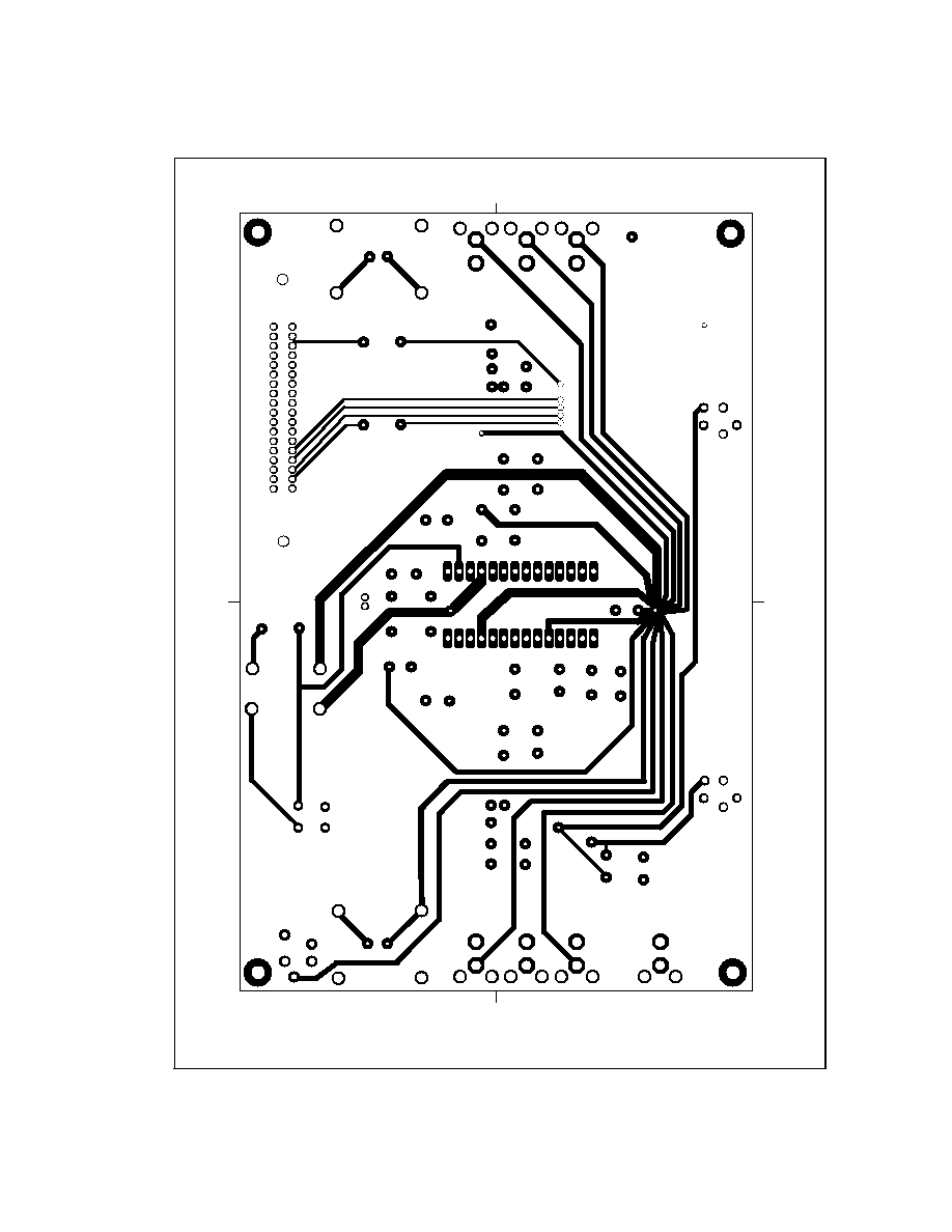
Typical Application PCB Layout (Bottom Layer)
DS100014-34
19
www.national.com
Typical Application PCB Layout (Top Layer)
DS100014-35
www.national.com
20
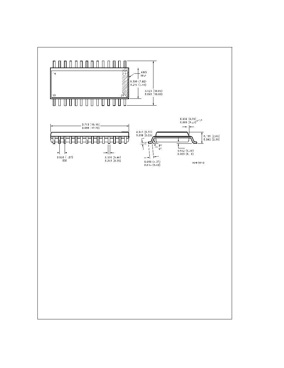
Physical Dimensions
inches (millimeters) unless otherwise noted
28-Lead SOIC Package (M28B)
Order Number LM4832M
NS Package Number M28B for SOIC
21
www.national.com
Physical Dimensions
inches (millimeters) unless otherwise noted (Continued)
LIFE SUPPORT POLICY
NATIONAL'S PRODUCTS ARE NOT AUTHORIZED FOR USE AS CRITICAL COMPONENTS IN LIFE SUPPORT DE-
VICES OR SYSTEMS WITHOUT THE EXPRESS WRITTEN APPROVAL OF THE PRESIDENT OF NATIONAL SEMI-
CONDUCTOR CORPORATION. As used herein:
1. Life support devices or systems are devices or sys-
tems which, (a) are intended for surgical implant into
the body, or (b) support or sustain life, and whose fail-
ure to perform when properly used in accordance
with instructions for use provided in the labeling, can
be reasonably expected to result in a significant injury
to the user.
2. A critical component in any component of a life support
device or system whose failure to perform can be rea-
sonably expected to cause the failure of the life support
device or system, or to affect its safety or effectiveness.
National Semiconductor
Corporation
Americas
Tel: 1-800-272-9959
Fax: 1-800-737-7018
Email: support@nsc.com
www.national.com
National Semiconductor
Europe
Fax: +49 (0) 1 80-530 85 86
Email: europe.support@nsc.com
Deutsch Tel: +49 (0) 1 80-530 85 85
English
Tel: +49 (0) 1 80-532 78 32
FranÁais Tel: +49 (0) 1 80-532 93 58
Italiano
Tel: +49 (0) 1 80-534 16 80
National Semiconductor
Asia Pacific Customer
Response Group
Tel: 65-2544466
Fax: 65-2504466
Email: sea.support@nsc.com
National Semiconductor
Japan Ltd.
Tel: 81-3-5620-6175
Fax: 81-3-5620-6179
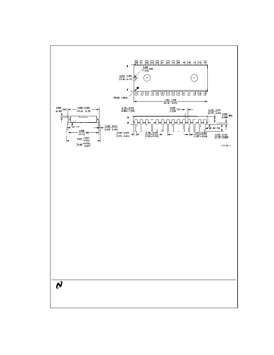
28-Lead Dual-In-Line Package (N28B)
Order Number LM4832N
NS Package Number N28B for DIP
LM4832
Digitally
Controlled
T
one
and
V
olume
Circuit
with
Stereo
Audio
Power
Amplifier
,
Microphone
Preamp
Stage
and
National
3D
Sound
National does not assume any responsibility for use of any circuitry described, no circuit patent licenses are implied and National reserves the right at any time without notice to change said circuitry and specifications.