 | ÐлекÑÑоннÑй компоненÑ: LM4834MSX | СкаÑаÑÑ:  PDF PDF  ZIP ZIP |
LM4834 1.75W Audio Power Amplifier with DC Volume Control and Microphone Preamp
LM4834
1.75W Audio Power Amplifier with DC Volume Control
and Microphone Preamp
General Description
The LM4834 is a monolithic integrated circuit that provides
DC volume control, and a bridged audio power amplifier ca-
pable of producing 1.75W into 4
with less than 1.0%
(THD). In addition, the headphone/lineout amplifier is ca-
pable of driving 70 mW into 32
with less than 0.1%(THD).
The LM4834 incorporates a volume control and an input mi-
crophone preamp stage capable of driving a 1 k
load im-
pedance.
Boomer
®
audio integrated circuits were designed specifically
to provide high quality audio while requiring a minimum
amount of external components in surface mount packaging.
The LM4834 incorporates a DC volume control, a bridged
audio power amplifier and a microphone preamp stage,
making it optimally suited for multimedia monitors and desk-
top computer applications.
The LM4834 features an externally controlled, low-power
consumption shutdown mode, and both a power amplifier
and headphone mute for maximum system flexibility and
performance.
Key Specifications
n
THD at 1.1W continuous average output power into 8
at 1kHz
0.5% (max)
n
Output Power into 4
at 1.0% THD+N
1.75W (typ)
n
THD at 70mW continuous average output power into
32
at 1kHz
0.1% (typ)
n
Shutdown Current
1.0µA (max)
n
Supply Current
17.5mA (typ)
Features
n
PC98 Compliant
n
"Click and Pop" suppression circuitry
n
Stereo line level outputs with mono input capability for
system beeps
n
Microphone preamp with buffered power supply
n
DC Volume Control Interface
n
Thermal shutdown protection circuitry
Applications
n
Multimedia Monitors
n
Desktop and Portable Computers
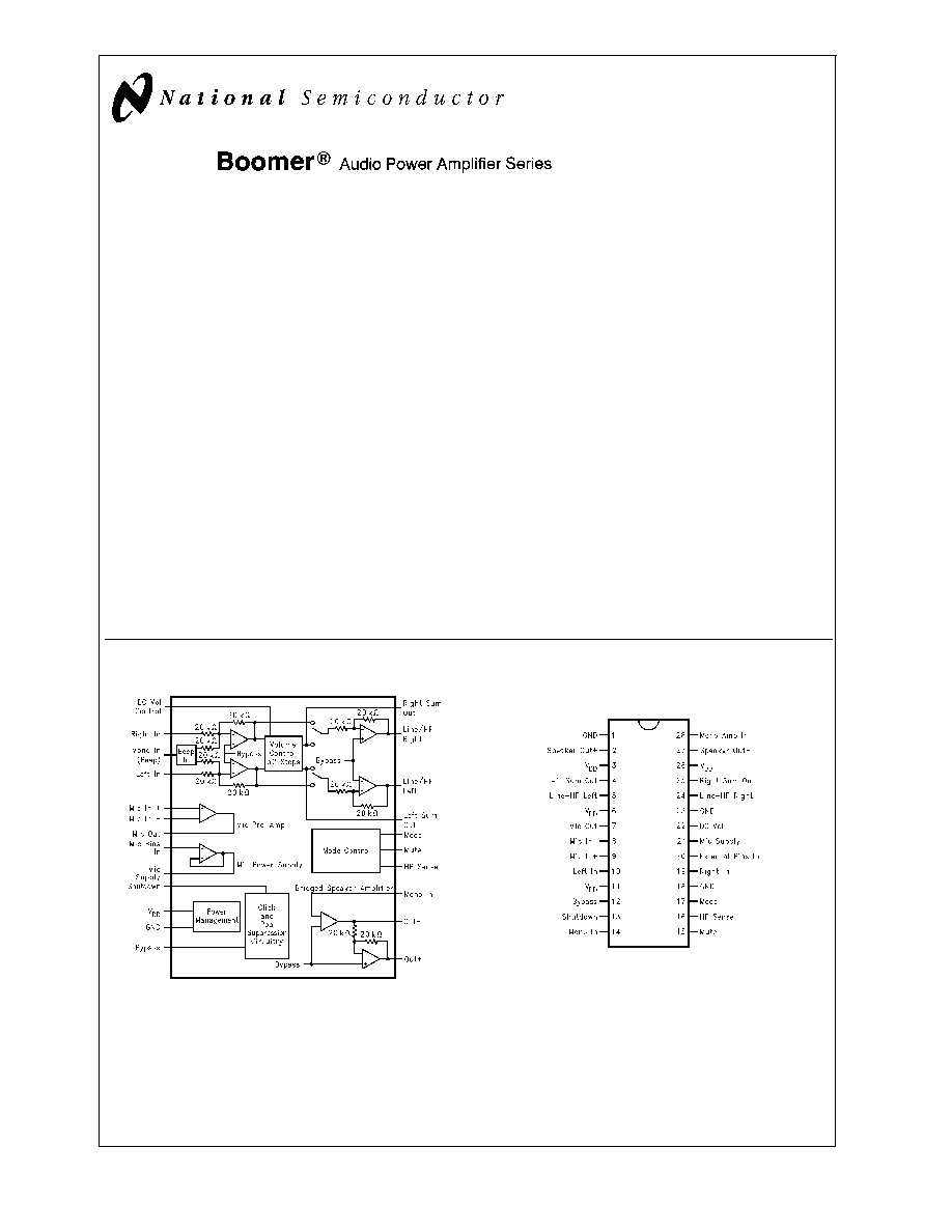
Block Diagram
Connection Diagram
Boomer
®
is a registered trademark of NationalSemiconductor Corporation.
DS100015-1
FIGURE 1. LM4834 Block Diagram
SSOP Package
DS100015-2
Top View
Order Number LM4834MS
See NS Package Number MSA028CB for SSOP
August 2000
LM4834
1.75W
Audio
Power
Amplifier
with
DC
V
olume
Control
and
Microphone
Preamp
© 2000 National Semiconductor Corporation
DS100015
www.national.com
Absolute Maximum Ratings
(Note 2)
If Military/Aerospace specified devices are required,
please contact the National Semiconductor Sales Office/
Distributors for availability and specifications.
Supply Voltage
6.0V
Storage Temperature
-65°C to +150°C
Input Voltage
-0.3V to V
DD
+0.3V
Power Dissipation
Internally limited
ESD Susceptibility (Note 4)
2000V
Pin 5
1500V
ESD Susceptibility (Note 5)
200V
Junction Temperature
150°C
Soldering Information
Small Outline Package
Vapor Phase (60 sec.)
215°C
Infrared (15 sec.)
220°C
See AN-450 "Surface Mounting and their Effects on
Product Reliability" for other methods of soldering
surface mount devices.
JC
(typ) -- MSA028CB
29°C/W
JA
(typ) -- MSA028CB
95°C/W
Operating Ratings
Temperature Range
T
MIN
T
A
T
MAX
-40°C
TA
85°C
Supply Voltage
4.5
V
DD
5.5V
Electrical Characteristics for Entire IC
(Notes 1, 2)
The following specifications apply for V
DD
= 5V unless otherwise noted. Limits apply for T
A
= 25°C.
Symbol
Parameter
Conditions
LM4834
Units
(Limits)
Typical
(Note 6)
Limit
(Note 7)
V
DD
Supply Voltage
4.5
V (min)
5.5
V (max)
I
DD
Quiescent Power Supply Current
V
IN
= 0V, I
O
= 0A
17.5
26
mA (max)
I
SD
Shutdown Current
V
pin13
= V
DD
0.6
2.0
µA (max)
Electrical Characteristics for Volume Attenuators
(Notes 1, 2)
The following specifications apply for V
DD
= 5V. Limits apply for T
A
= 25°C.
Symbol
Parameter
Conditions
LM4834
Units
(Limits)
Typical
(Note 6)
Limit
(Note 7)
C
RANGE
Attenuator Range
Gain with V
pin 22
= 5V
2.6
3.65
dB (max)
Attenuation with V
pin 22
= 0V
-75
-88
dB (min)
A
M
Mute Attenuation
V
pin 15
= 5V, Sum Out
-92
-105
dB (max)
V
pin 15
= 5V, Line Out/Headphone
Amp
-92
-105
dB (max)
Electrical Characteristics for Microphone Preamp and Power Supply
(Notes 1, 2)
The following specifications apply forV
DD
= 5V unless otherwise noted. Limits apply for T
A
= 25°C.
Symbol
Parameter
Conditions
LM4834
Units
(Limits)
Typical
(Note 6)
Limit
(Note 7)
V
OS
Offset Voltage
V
IN
= 0V
0.9
mV
SNR
Signal to Noise Ratio
V
DD
= 5V, R
L
= 1k, f = 1 kHz, V
OUT
=
4.7V, A-Wtd Filter
123
dB
V
SWING
Output Voltage Swing
f = 1 kHz, THD
<
1.0%, R
L
= 1 k
4.72
V
E
NO
Input Referred Noise
A-Weighted Filter
1.2
µV
PSRR
Power Supply Rejection Ratio
f = 120 Hz, V
RIPPLE
= 200 mVrms,
C
B
=1µF
28
dB
V
S
Mic Power Supply
R
L
= 1 k
, Bias In = 2.5V
2.5
2.5
V (min)
LM4834
www.national.com
2
Electrical Characteristics for Line/Headphone Amplifier
(Notes 1, 2)
The following specifications apply for V
DD
= 5V. Limits apply for T
A
= 25°C.
Symbol
Parameter
Conditions
LM4834
Units
(Limits)
Typical
(Note 6)
Limit
(Note 7)
P
O
Output Power
THD = 0.1%; f = 1kHz; R
L
= 32
70
mW
THD = 10%; f = 1 kHz; R
L
= 32
95
mW
THD+N
Total Harmonic Distortion+Noise
V
OUT
= 4V
P-P
, 20 Hz
<
f
<
20 kHz,
R
L
= 10k
, A
VD
= -1
0.05
%
PSRR
Power Supply Rejection Ratio
C
B
= 1.0 µF, f =120 Hz,
V
RIPPLE
= 200 mVrms
30
dB
SNR
Signal to Noise Ratio
V
DD
=5V, P
OUT
=75mW, R
L
= 32
,
A-Wtd Filter
102
dB
Electrical Characteristics for Bridged Speaker Amplifer
(Notes 1, 2)
The following specifications apply for V
DD
= 5V, unless otherwise noted. Limits apply for T
A
= 25°C.
Symbol
Parameter
Conditions
LM4834
Units
(Limits)
Typical
(Note 6)
Limit
(Note 7)
V
OS
Output Offset Voltage
V
IN
= 0V
5
30
mV (max)
P
O
Output Power
THD = 0.5% (max);f = 1 kHz;
R
L
= 8
1.1
1.0
W (min)
THD+N = 10%;f = 1 kHz; R
L
= 8
1.5
W
THD+N
Total Harmonic Distortion+Noise
P
O
= 1W, 20 Hz
<
f
<
20 kHz,
R
L
= 8
, A
VD
= 2
0.3
%
P
O
= 340 mW, R
L
= 32
1.0
%
PSRR
Power Supply Rejection Ratio
C
B
= 1.0 µF, f = 120 Hz,V
RIPPLE
=
200 mVmrs
58
dB
SNR
Signal to Noise Ratio
V
DD
= 5V, P
OUT
= 1.1W, R
L
= 8
,
A-Wtd Filter
93
dB
Note 1: All voltages are measured with respect to the ground pins, unlessotherwise specified. All specifications are tested using the typical application as shown in
Figure 1
.
Note 2:
Absolute Maximum Ratings
indicate limits beyond which damage to the device may occur.
Operating Ratings
indicate conditionsfor which the device is func-
tional, but do not guarantee specific performance limits.
Electrical Characteristics
state DC and AC electrical specifications under particular test conditions which guar-
antee specific performance limits. This assumes that the deviceis within the Operating Ratings. Specifications are not guaranteed for parameters where no limit is
given, however, the typical value is a good indication of device performance.
Note 3: The maximum power dissipation must be derated at elevated temperatures and is dictated by T
JMAX
,
JA
, and the ambient temperature T
A
. The maximum
allowable power dissipation is P
DMAX
= (T
JMAX
- T
A
)/
JA
.For the LM4834MS, T
JMAX
= 150°C, and the typical junction-to-ambient thermal resistance, when board
mounted, is 95°C/W assuming the MSA028CB package.
Note 4: Human body model, 100 pF discharged through a 1.5 k
resistor.
Note 5: Machine Model, 220 pF240 pF discharged through all pins.
Note 6: Typicals are measured at 25°C and represent the parametric norm.
Note 7: Limits are guaranteed to National's AOQL (Average Outgoing Quality Level).
LM4834
www.national.com
3
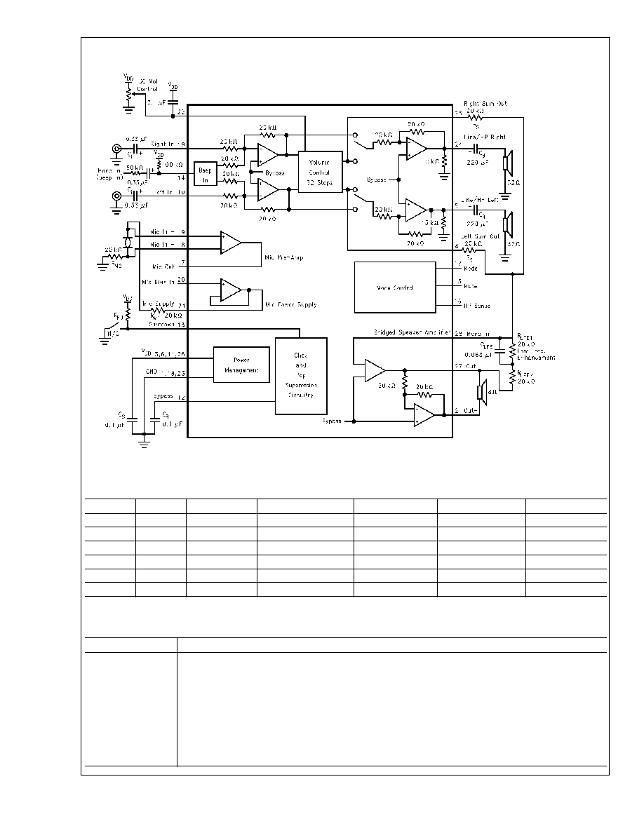
Typical Application
Truth Table for Logic Inputs
Mode
Mute
HP Sense
DC Vol. Control
Line/HP Left
Line/HP Right
Speaker Out
0
0
0
Adjustable
Fixed Level
Fixed Level
Vol. Changes
0
0
1
Adjustable
Fixed Level
Fixed Level
Muted
0
1
X
_
Fixed Level
Fixed Level
Muted
1
0
0
Adjustable
Vol. Changes
Vol. Changes
Vol. Changes
1
0
1
Adjustable
Vol. Changes
Vol. Changes
Muted
1
1
X
_
Muted
Muted
Muted
External Components Description
Figure 2
Components.
Functional Description
1.
C
i
Input coupling capacitor which blocks the DC voltage at the amplifier's input terminals. Also creates a
high pass filter with R
i
at f
c
= 1/(2
R
i
C
i
). Refer to the section, Proper Selection of External
Components, for an explanation of how to determine the value of C
i
.
2.
C
S
Supply bypass capacitor which provides power supply filtering. Refer to the Power Supply Bypassing
section for information concerning proper placement and selection of the supply bypass capacitor.
3.
C
B
Bypass pin capacitor which provides half-supply filtering. Refer to the section, Proper Selection of
External Components, for information concerning proper placement and selection of C
B
.
4.
C
O
Output coupling capacitor which blocks the DC voltage at the amplifiers output. Forms a high pass filter
with R
L
at f
o
= 1/(2
R
L
C
O
).
DS100015-3
FIGURE 2. Typical Application Circuit
LM4834
www.national.com
4
External Components Description
Figure 2 (Continued)
Components.
Functional Description
5.
R
S
Summing resistor that combines the right and left line level outputs into the mono input of the bridged
amplifier. The two summing resistors in parallel determine the value of the input resistance of the bridged
amplifier.
6.
R
LFE
Resistor for the bridged power amplifier in series with R
F
at high frequencies. Used in conjunction with
C
LFE
to increase closed-loop gain at low frequencies.
7.
R
F
Feedback resistor which sets the closed-loop gain in conjunction with the equivalent R
S
for the bridged
power amplifier.
8.
R
M1
Resistor in series with Microphone supply pin and the microphone for biasing differential input
microphones.
9.
R
M2
Resistor in series with reference ground and the microphone used for biasing differential input
microphones.
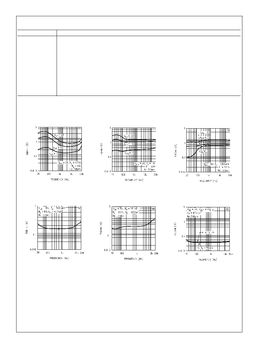
Typical Performance Characteristics
THD+N vs Frequency
Bridged Power Amp
DS100015-5
THD+N vs Frequency
Bridged Power Amp
DS100015-4
THD+N vs Frequency
Bridge Power Amp
DS100015-6
THD+N vs Frequency
Line Out/HP Amplifiers
DS100015-7
THD+N vs Frequency
Line Out/HP Amplifiers
DS100015-8
THD+N vs Frequency
Line Out/HP Amplifiers
DS100015-9
LM4834
www.national.com
5