LM4845
Output Capacitor-less Audio Subsystem with
Programmable National 3D
General Description
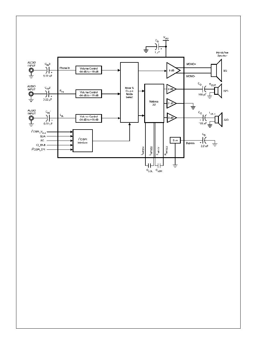
The LM4845 is an audio power amplifier capable of deliver-
ing 500mW of continuous average power into a mono 8
bridged-tied load (BTL) with 1% THD+N, 25mW per channel
of continuous average power into stereo 32
single-ended
(SE) loads with 1% THD+N, or an output capacitor-less
(OCL) configuration with identical specification as the SE
configuration, from a 3.3V power supply.
The LM4845 features a 32-step digital volume control and
eight distinct output modes. The digital volume control, 3D
enhancement, and output modes (mono/SE/OCL) are pro-
grammed through a two-wire I
2
C or a three-wire SPI com-
patible interface that allows flexibility in routing and mixing
audio channels. The LM4845 has three input channels: one
pair for a two-channel stereo signal and the third for a
single-channel mono input.
The LM4845 is designed for cellular phone, PDA, and other
portable handheld applications. It delivers high quality output
power from a surface-mount package and requires only
seven external components in the OCL mode (two additional
components in SE mode).
Key Specifications
j
THD+N at 1kHz, 500mW
into 8
BTL (3.3V)
1.0% (typ)
j
THD+N at 1kHz, 25mW
into 32
SE (3.3V)
1.0% (typ)
j
Single Supply Operation (V
DD
)
2.7 to 5.5V
j
I
2
C/SPI Single Supply Operation
2.2 to 5.5V
Features
n
I
2
C/SPI Control Interface
n
I
2
C/SPI programmable National 3D Audio
n
I
2
C/SPI controlled 32 step digital volume control (-54dB
to +18dB)
n
Three independent volume channels (Left, Right, Mono)
n
Eight distinct output modes
n
microSMD surface mount packaging
n
"Click and Pop" suppression circuitry
n
Thermal shutdown protection
n
Low shutdown current (0.1uA, typ)
Applications
n
Moblie Phones
n
PDAs
Boomer
Æ
is a registered trademark of National Semiconductor Corporation.
March 2005
LM4845
Output
Capacitor-less
Audio
Subsystem
with
Programmable
National
3D
© 2005 National Semiconductor Corporation
DS201059
www.national.com
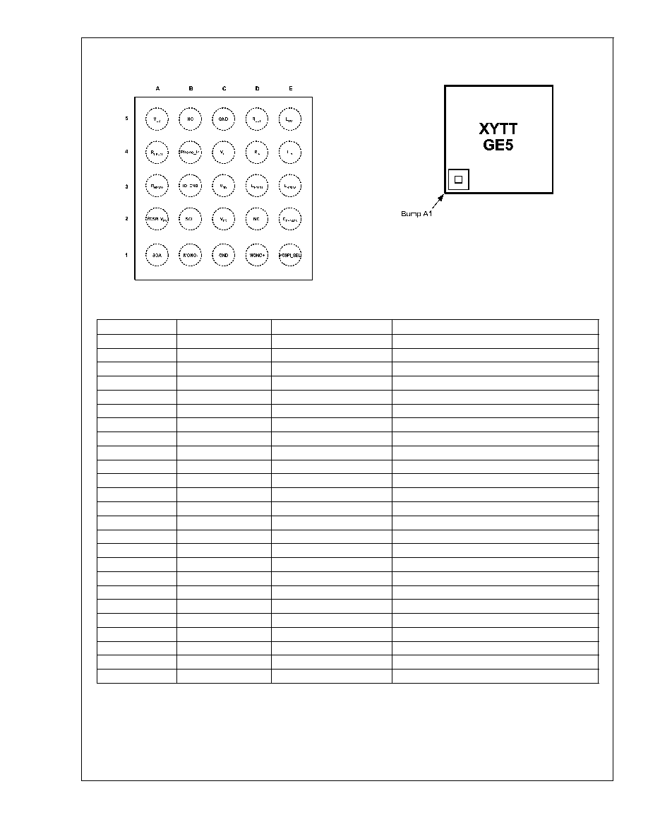
Connection Diagrams
25-Bump micro SMD
201059K1
Top View
201059K0
Top View
XY - Date Code
TT - Die Traceability
G - Boomer Family
E5 - LM4845ITL
Bump
Name
Description
1
A1
SDA
I
2
C or SPI Data
2
A2
I
2
CSPIV
DD
I
2
C or SPI Interface Power Supply
3
A3
R
HP3D2
Right Headphone 3D Input 2
4
A4
R
HP3D1
Right Headphone 3D Input 1
5
A5
VOC
Center Amplifier Output
6
B1
Mono-
Loudspeaker Negative Output
7
B2
SCL
I
2
C or SPI Clock
8
B3
ID_ENB
Address Identification/Enable Bar
9
B4
Phone_In
Mono Input
10
B5
NC
No Connect
11
C1
GND
Ground
12
C2
V
DD
Power Supply
13
C3
V
DD
Power Supply
14
C4
V
DD
Power Supply
15
C5
GND
GND
16
D1
Mono+
Loudspeaker Positive Output
17
D2
NC
No Connect
18
D3
L
HP3D1
Left Headphone 3D Input 1
19
D4
R
IN
Right Input Channel
20
D5
R
OUT
Right Headphone Output
21
E1
I
2
C SPI_SEL
I
2
C or SPI Select
22
E2
C
BYPASS
Half-Supply Bypass
23
E3
L
HP3D2
Left Headphone 3D Input 2
24
E4
L
IN
Left Input Channel
25
E5
L
OUT
Left Headphone Output
LM4845
www.national.com
4
Absolute Maximum Ratings
(Note 2)
If Military/Aerospace specified devices are required,
please contact the National Semiconductor Sales Office/
Distributors for availability and specifications.
Supply Voltage
6.0V
Storage Temperature
-65∞C to +150∞C
ESD Susceptibility (Note 3)
2.0kV
ESD Machine model (Note 6)
200V
Junction Temperature (T
J
)
150∞C
Solder Information (Note 1)
Vapor Phase (60 sec.)
215∞C
Infrared (15 sec.)
220∞C
Thermal Resistance
JA
(typ) - TLA25CBA
65∞C/W (Note 8)
Operating Ratings
(Note 2)
Temperature Range
-40∞C to 85∞C
Supply Voltage (V
DD
)
2.7V
V
DD
5.5V
Supply Voltage (I
2
C/SPI)
2.2V
V
DD
5.5V
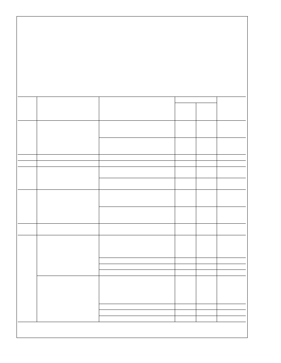
Electrical Characteristics 3.3V
(Notes 2, 7)
The following specifications apply for V
DD
= 3.3V, T
A
= 25∞C unless otherwise specified. [A
V
= 2 (BTL), A
V
= 1 (SE)]
Symbol
Parameter
Conditions
LM4845
Units
(Limits)
Typical
(Note 4)
Limits
(Note 5)
I
DD
Supply Current
Output Modes 2, 4, 6
V
IN
= 0V; No load,
OCL = 0 (Table 2)
3.3
6.5
mA (max)
Output Modes 1, 3, 5, 7
V
IN
= 0V; No load, BTL,
OCL = 0 (Table 2)
6
11
mA (max)
I
SD
Shutdown Current
Output mode 0
0.1
1
µA (max)
V
OS
Output Offset Voltage
V
IN
= 0V, Mode 5 (Note 10)
10
50
mV (max)
P
O
Output Power
SPKR
OUT
; R
L
= 8
THD+N = 1%; f = 1kHz, BTL, Mode 1
500
400
mW (min)
R
OUT
and L
OUT
; R
L
= 32
THD+N = 1%; f = 1kHz, SE, Mode 4
30
20
mW (min)
THD+N
Total Harmonic Distortion Plus
Noise
SPKR
OUT
f = 20Hz to 20kHz
P
OUT
= 250mW; R
L
= 8
, BTL, Mode 1
0.5
%
R
OUT
and L
OUT
f = 20Hz to 20kHz
P
OUT
= 12mW; R
L
= 32
, SE, Mode 4
0.5
%
N
OUT
Output Noise
A-weighted (Note 9), Mode 5, BTL
input referred
26
µV
PSRR
Power Supply Rejection Ratio
SPKR
OUT
V
RIPPLE
= 200mV
PP
; f = 217Hz,
C
B
= 2.2µF, BTL
All audio inputs terminated into 50
;
Output referred Gain (BTL) = 6dB
Output Mode 1,7
71
dB
Output Mode 3
68
dB
Output Mode 5
63
dB
Power Supply Rejection Ratio
R
OUT
and L
OUT
V
RIPPLE
= 200mV
PP
; f = 217Hz
C
B
= 2.2µF, SE, C
O
= 100µF
All audio inputs terminated into 50
;
Output referred Gain,
OCL = 0 (Table 2)
Output Mode 2
88
dB
Output Mode 4
88
dB
Output Mode 6, 7
84
dB
LM4845
www.national.com
5