LM4854
1.9W Monaural, 85mW Stereo Headphone Audio
Amplifier
General Description
The unity-gain stable LM4854 is both a mono differential
output (for bridge-tied loads, or BTL) audio power amplifier
and a single-ended (SE) stereo headphone amplifier. Oper-
ating on a single 5V supply, the mono BTL mode delivers
1.1W (typ) to an 8
load, 1.7W (typ) to a 4 load (Note 1) at
1% THD+N. In SE stereo mode, the amplifier will deliver
85mW to 32
loads. The LM4854 features a new circuit
topology that suppresses output transients ('click and pops')
and eliminates SE-mode output coupling capacitors, saving
both component and board space costs. The LM4854 has
three inputs: one pair for a two-channel stereo signal and the
third for a single-channel mono input.
The LM4854 is designed for PDA, cellular telephone, note-
book, and other handheld portable applications. It delivers
high quality output power from a surface-mount package and
requires few external components. Other features include an
active-low micropower shutdown mode, an "instant-on" low
power standby mode, and thermal shutdown protection.
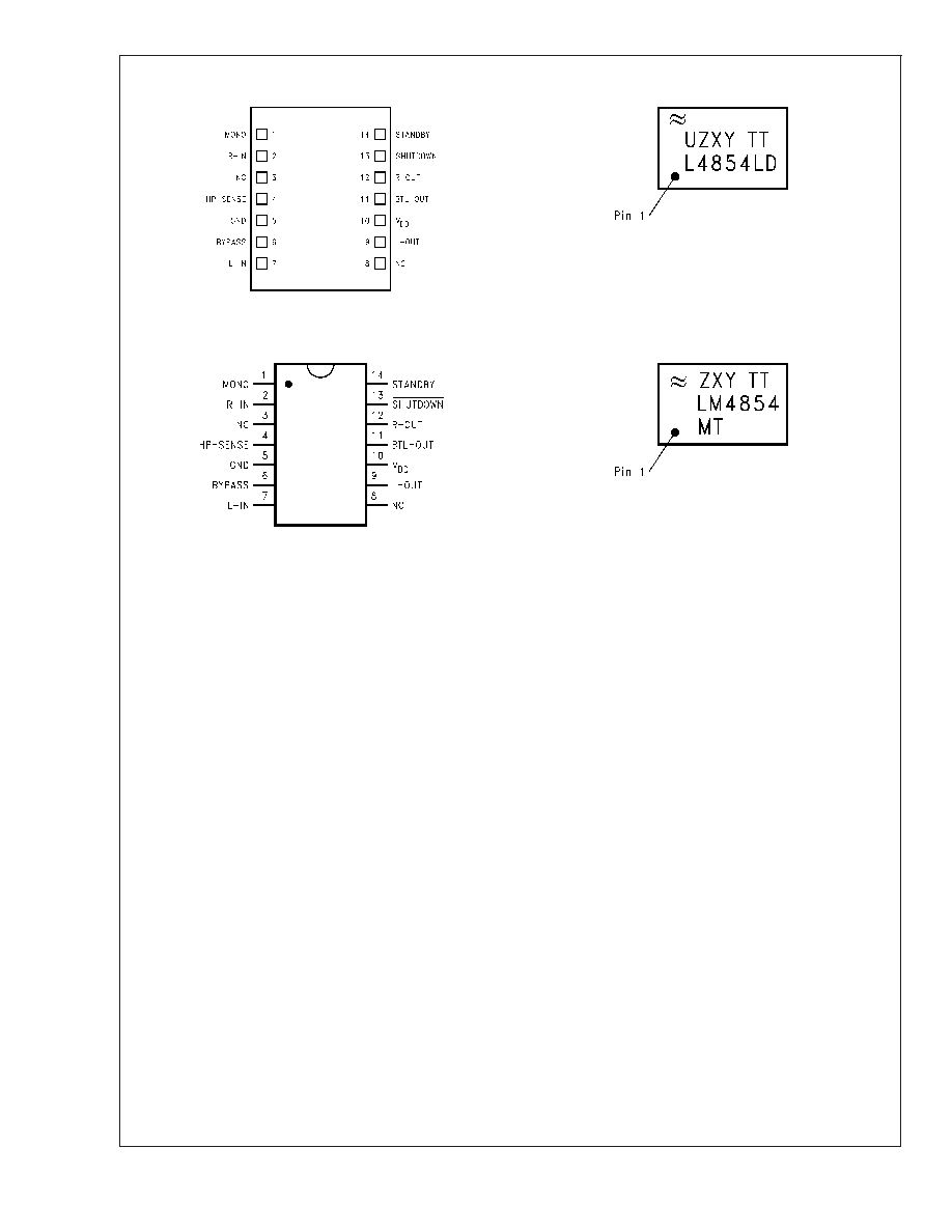
The LM4854 is available in the very space-efficient 12-lead
micro SMD, exposed-DAP LLP for higher power applica-
tions, and TSSOP packages.
Note 1: An LM4854LD that has been properly mounted to a circuit board will
deliver 1.7W (typ) into a 4
load.
Key Specifications
j
LLP BTL output power (R
L
= 3.2
and
THD+N = 1%)
V
DD
= 3.0V
1.0W (typ)
V
DD
= 5.0V
1.9W (typ)
j
LLP BTL output power (R
L
= 4
and
THD+N = 1%)
V
DD
= 3.0V
900mW (typ)
V
DD
= 5.0V
1.7W (typ)
j
LLP BTL output power (R
L
= 8
and
THD+N = 1%)
V
DD
= 3.0V
380mW (typ)
V
DD
= 5.0V
1.1W (typ)
j
SE output power (R
L
= 32
and THD+N
= 1.0%)
V
DD
= 3.0V
32mW (typ)
V
DD
= 5.0V
93mW (typ)
j
Micropower shutdown supply current
V
DD
= 3.0V
0.005µA (typ)
V
DD
= 5.0V
0.05µA (typ)
j
Standby supply current
V
DD
= 3.0V
16µA (typ)
V
DD
= 5.0V
27µA (typ)
j
PSRR (f = 1kHz, 3.0V
V
DD
5.0V,
(Fig. 1))
BTL
60dB (typ)
SE
66dB (typ)
Features
n
Fast 0.1ms (typ) and 1.0ms (max) turn-on and turn-off
time
n
Eliminates SE amplifier output coupling capacitors
n
Advanced "click and pop" suppression circuitry
n
Stereo headphone amplifier mode
n
Low-power standby and ultra-low current micropower
shutdown modes
n
Thermal shutdown protection circuitry
n
2.4V to 5.5V operation
n
Unity-gain stable
n
Gain set with external resistors
n
Space-saving micro SMD package, exposed-DAP LLP,
and TSSOP
Applications
n
PDAs
n
Notebook computers
n
Cellular phones
n
Handheld portable electronic devices
Boomer
Æ
is a registered trademark of National Semiconductor Corporation.
April 2003
LM4854
1.9W
Monaural,
85mW
Stereo
Headphone
Audio
Amplifier
© 2003 National Semiconductor Corporation
DS200382
www.national.com
Absolute Maximum Ratings
(Notes 2,
3)
If Military/Aerospace specified devices are required,
please contact the National Semiconductor Sales Office/
Distributors for availability and specifications.
Supply Voltage
6.0V
Storage Temperature
-65∞C to +150∞C
Input Voltage
-0.3V to V
DD
+ 0.3V
Power Dissipation(Note 4)
Internally Limited
ESD Susceptibility (Note 5)
All pins except Pin C3 (IBL), Pin11
(LD/MT)
2000V
Pin C3 (IBL), Pin 11 (LD/MT)
8000V
ESD Susceptibility(Note 6)
200V
Junction Temperature (T
J
)
150∞C
Solder Information
Small Outline Package
Vapor Phase (60 sec.)
215∞C
Infrared (15 sec.)
220∞C
See AN-540 "Surface Mounting and
their Effects on Product Reliability"
for other methods of soldering
surface-mount devices.
Thermal Resistance
JA
(typ) -- BLA12BAB
121∞C/W
JC
(typ) -- LDA14A
3∞C/W
JA
(typ) -- LDA14A
42∞C/W (Note 7)
JC
(typ) -- MTC14
40∞C/W
JA
(typ) -- MTC14
109∞C/W
Operating Ratings
(Note 3)
Temperature Range
T
MIN
T
A
T
MAX
-40∞C
T
A
+85∞C
Supply Voltage
2.4V
V
DD
5.5V
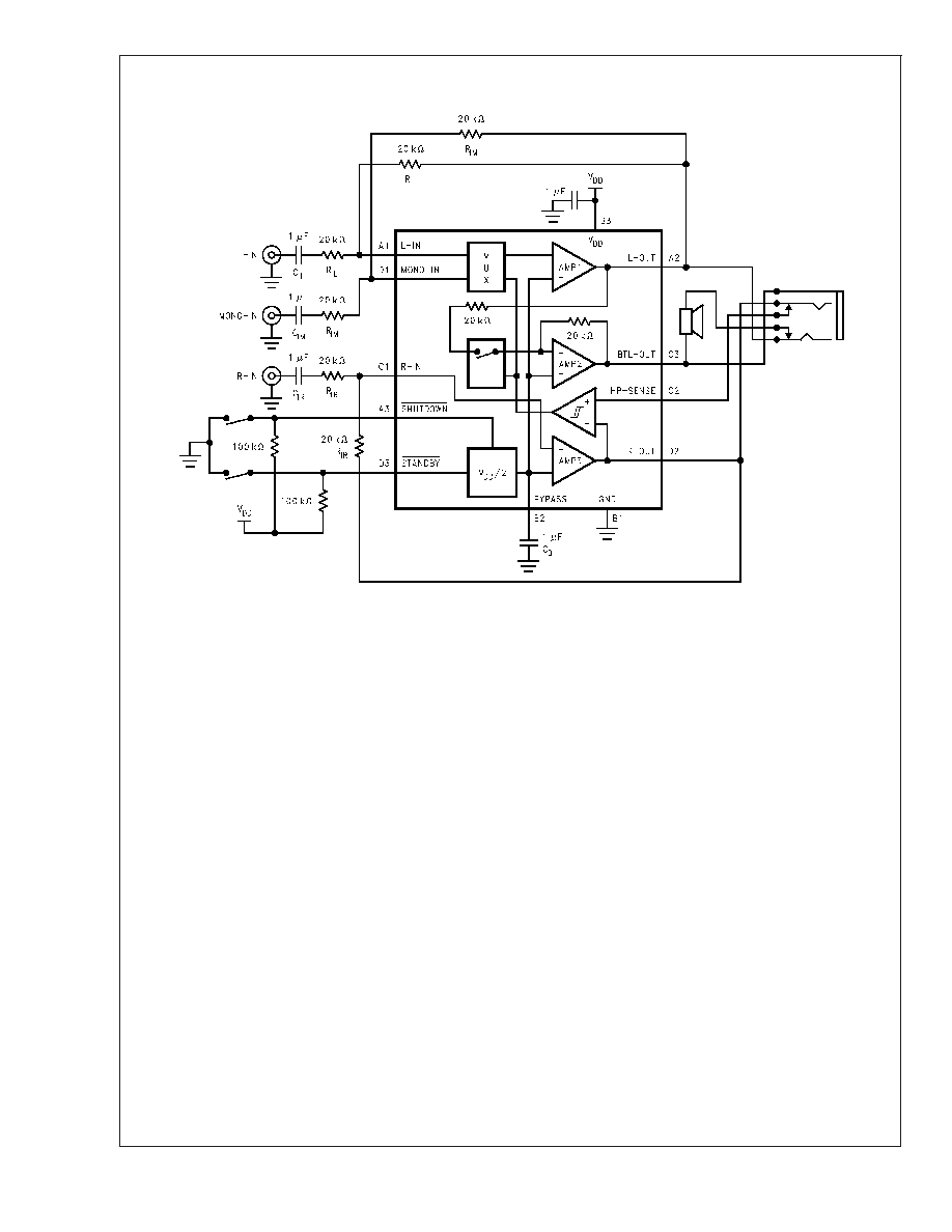
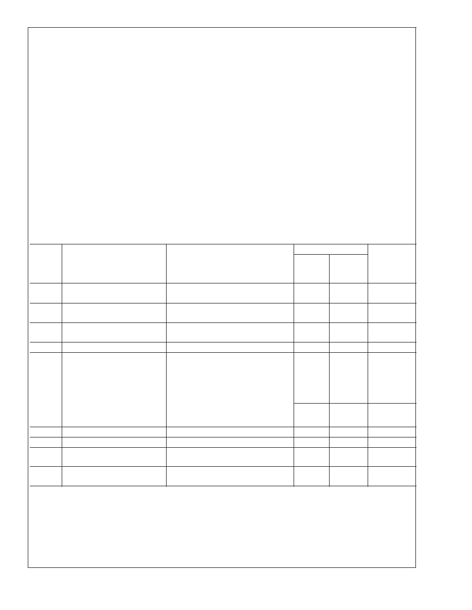
Electrical Characteristics for Entire Amplifier (V
DD
= 5V)
The following specifications apply for circuit shown in Figure 1, unless otherwise specified. Limits apply for T
A
= 25∞C.
Symbol
Parameter
Conditions
LM4854
Units
(Limits)
Typical
(Note 8)
Limit
(Notes 9,
10)
I
DD
Quiescent Power Supply Current
V
IN
= 0V; I
O
= 0A, No Load
5.0
12
mA max)
V
IN
= 0V; I
O
= 0A, 8
Load
6.5
15
mA (max)
I
STBY
Standby Quiescent Power Supply
Current
V
STANDBY
= GND
27
35
µA (max)
I
SD
Shutdown Quiescent Power
Supply Current
V
SHUTDOWN
= GND
0.05
0.2
µA (max)
V
OS
Output Offset Voltage
8
Load
2.0
40
mV (max)
PSRR
Power Supply Rejection Ratio
C
BYPASS
= 1.0µF, R
SOURCE
= 10
V
RIPPLE
= 200mV
p-p
sinewave
BTL, R
L
= 8
, R
IN
= 10
f
IN
= 217Hz
f
IN
= 1kHz
SE, R
L
= 32
, R
IN
= 10
f
IN
= 217Hz
f
IN
= 1kHz
61
63
dB
dB
68
71
dB
dB
t
RSH
Return-from-Shutdown Time
C
BYPASS
= 1.0µF
200
ms
t
RST
Return-from-Standby Time
0.1
1.0
ms(max)
V
IH
Shutdown or Standby Logic High
Treshold
1.4
V (min)
V
IL
Shutdown or Standby Logic Low
Treshold
0.4
V (max)
LM4854
www.national.com
5