 | ÐлекÑÑоннÑй компоненÑ: LM4856ITL | СкаÑаÑÑ:  PDF PDF  ZIP ZIP |
Äîêóìåíòàöèÿ è îïèñàíèÿ www.docs.chipfind.ru
LM4856
Integrated Audio Amplifier System
General Description
The LM4856 is an audio power amplifier system capable of
delivering 1.1W (typ) of continuous average power into a
mono 8
bridged-tied load (BTL) with 1% THD+N and
60mW (typ) per channel of continuous average power into
stereo 32
single-ended (SE) loads with 0.5% THD+N, us-
ing a 5V power supply.
The LM4856 features a 32 step digital volume control and
eight distinct output modes. The digital volume control and
output modes are programmed through a two-wire I
2
C com-
patible control interface, that allows flexibility in routing and
mixing audio channels.
The LM4856 is designed for cellular phone, PDA, and other
portable handheld applications. It delivers high quality output
power from a surface-mount package and requires only
eight external components.
The industry leading micro SMD package only utilizes 2mm
x 2.3mm of PCB space, making the LM4856 the most space
efficient audio sub system available today.
Key Specifications
n
THD+N at 1kHz, 1.1W into 8
BTL
1.0% (typ)
n
THD+N at 1kHz, 60mW into 32
SE
0.5% (typ)
n
Single Supply Operation
2.6 to 5.0V
Features
n
1.1W (typ) output power with 8
mono BTL load
n
60mW (typ) output power with stereo 32
SE loads
n
I
2
C programmable 32 step digital volume control
n
Eight distinct output modes
n
micro-SMD and LLP surface mount packaging
n
"Click and Pop" suppression circuitry
n
Thermal shutdown protection
n
Low shutdown current (0.1uA, typ)
Applications
n
Moblie Phones
n
PDAs
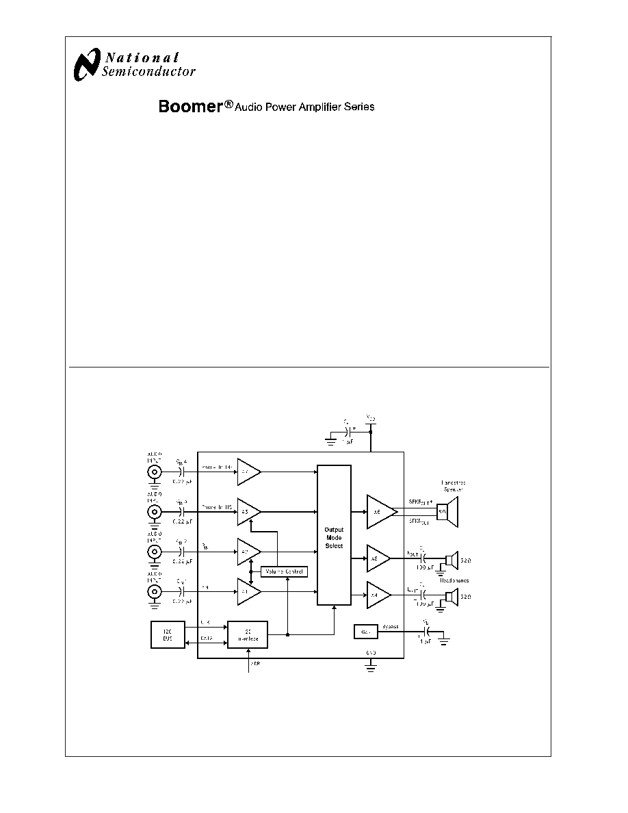
Typical Application
Boomer
®
is a registered trademark of National Semiconductor Corporation.
20060732
FIGURE 1. Typical Audio Amplifier Application Circuit
May 2004
LM4856
Integrated
Audio
Amplifier
System
© 2004 National Semiconductor Corporation
DS200607
www.national.com
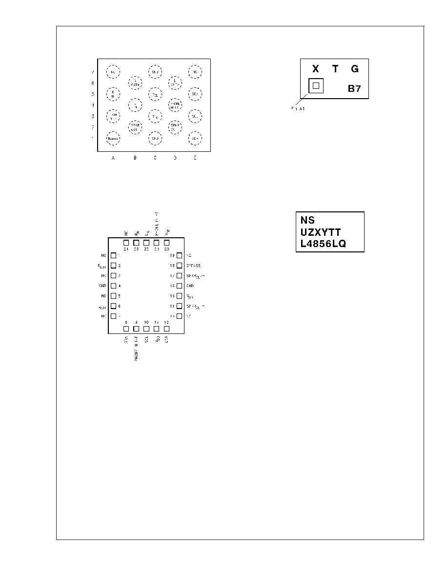
Connection Diagrams
18-Bump micro SMD Marking (ITL)
200607A9
Top View
(Bump-side down)
Order Number LM4856ITL
See NS Package Number TLA18AAA
200607E4
Top View
X - Date Code
T - Die Traceability
G - Boomer Family
B7 - LM4856ITL
LLP Package
18 Lead LLP Marking
200607D3
Top View
Order Number LM4856LQ
See NS Package Number LQA24A for Exposed-DAP LLP
20060701
Top View
NS - Std NS Logo
U - Wafer Fab Code
Z - Assembly Plant Code
XY - 2 Digit Date Code
TT - Die Run Traceability
L4856LQ - LM4856LQ
LM4856
www.national.com
2
Absolute Maximum Ratings
(Note 2)
If Military/Aerospace specified devices are required,
please contact the National Semiconductor Sales Office/
Distributors for availability and specifications.
Supply Voltage
6.0V
Storage Temperature
-65°C to +150°C
ESD Susceptibility (Note 4)
2.0kV
ESD Machine model (Note 7)
200V
Junction Temperature (T
J
)
150°C
Solder Information (Note 1)
Vapor Phase (60 sec.)
215°C
Infrared (15 sec.)
220°C
Thermal Resistance
JA
(typ) - LQA24A
42°C/W
JC
(typ) - LQA24A
3.0°C/W
JA
(typ) - TLA18AAA
48°C/W (Note 9)
JC
(typ) - TLA18AAA
23°C/W (Note 9)
Operating Ratings
(Note 3)
Temperature Range
-40°C to 85°C
Supply Voltage V
DD
2.6V
V
DD
5.0V
Note 1: See AN-450 "Surface Mounting and their effects on Product Reli-
ability" for other methods of soldering surface mount devices.
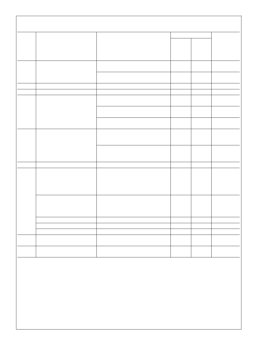
Electrical Characteristics
(Notes 3, 8)
The following specifications apply for V
DD
= 5.0V, T
A
= 25°C unless otherwise specified.
Symbol
Parameter
Conditions
LM4856
Units
(Limits)
Typical
(Note 5)
Limits
(Notes 6,
11)
I
DD
Supply Current
Output modes 1, 2, 3, 4, 5, 6, 7
V
IN
= 0V; No loads
7.5
11
mA (max)
Output modes 1, 2, 3, 4, 5, 6, 7
V
IN
= 0V; Loaded (Figure 1)
8.5
12
mA (max)
I
SD
Shutdown Current
Output mode 0
0.1
2.0
µA (max)
V
OS
Output Offset Voltage
V
IN
= 0V
5.0
40
mV (max)
P
O
Output Power
SPKR
OUT
; R
L
= 4
THD+N = 1%; f = 1kHz, LM4856LQ
1.5
W
SPKR
OUT
; R
L
= 8
THD+N = 1%; f = 1kHz
1.1
0.8
W (min)
R
OUT
and L
OUT
; R
L
= 32
THD+N = 0.5%; f = 1kHz
60
45
mW (min)
THD+N
Total Harmonic Distortion Plus
Noise
SPKR
OUT
f = 20Hz to 20kHz
P
OUT
= 400mW; R
L
= 8
0.5
%
R
OUT
and L
OUT
f = 20Hz to 20kHz
P
OUT
= 15mW; R
L
= 32
0.5
%
N
OUT
Output Noise
A-weighted (Note 10)
29
µV
PSRR
Power Supply Rejection Ratio
SPKR
OUT
V
RIPPLE
= 200mV
PP
; f = 217Hz,
C
B
= 1.0µF
All audio inputs terminated into 50
;
Output referred Gain (BTL) = 12dB
Output Mode 1, 3, 5, 7
58
54
dB (min)
Power Supply Rejection Ratio
R
OUT
and L
OUT
V
RIPPLE
= 200mV
PP
; f = 217Hz
C
B
= 1.0µF
All audio inputs terminated into 50
;
Output referred Maximum gain setting
Output Mode 2, 3
68
59
dB (min)
Output Mode 4, 5
60
54
dB (min)
Output Mode 6, 7
56
51
dB (min)
V
IH
Logic High Input Voltage
0.7 x V
DD
V
DD
V (min)
V (max)
LM4856
www.national.com
3
Electrical Characteristics
(Notes 3, 8) (Continued)
The following specifications apply for V
DD
= 5.0V, T
A
= 25°C unless otherwise specified.
Symbol
Parameter
Conditions
LM4856
Units
(Limits)
Typical
(Note 5)
Limits
(Notes 6,
11)
V
IL
Logic Low Input Voltage
0.4
GND
V (max)
V (min)
Digital Volume Range
(R
IN
and L
IN
)
Input referred minimum gain
-34.5
-35.1
-33.9
dB (min)
dB (max)
Input referred maximum gain
12.0
11.4
12.6
dB (min)
dB (max)
Digital Volume Range
(Phone_In_HS)
Input referred minimum gain
-40.5
-41.1
-39.9
dB (min)
dB (max)
Input referred maximum gain
6.0
5.4
6.6
dB (min)
dB (max)
Digital Volume Stepsize
1.5
dB
Digital Volume Stepsize Error
±
0.1
±
0.6
dB ( max)
Phone_In_IHF Volume
BTL gain from Phone_In _IHF to
SPKR
OUT
12
11.4
12.6
dB (min)
dB (max)
Phone_In_IHF Mute Attenuation
Output Mode 2, 4, 6
100
dB
Phone_In_IHF Input Impedance
20
15
25
k
(min)
k
(max)
Phone_In_HS Input Impedance
Maximum gain setting
33.5
25
42
k
(min)
k
(max)
Mininum gain setting
100
75
125
k
(min)
k
(max)
R
IN
and L
IN
Input Impedance
Maximum gain setting
20
15
25
k
(min)
k
(max)
Mininum gain setting
100
75
125
k
(min)
k
(max)
T
SD
Thermal Shutdown Temperature
170
150
°C (min)
t
1
SCL (Clock) Period
2.5
µs (min)
t
2
SDA to SCL Set-up Time
100
ns (min)
t
3
Data Out Stable Time
0
ns (min)
t
4
Start Condition Time
100
ns (min)
t
5
Stop Condition Time
100
ns (min)
LM4856
www.national.com
4
Electrical Characteristics
(Notes 2, 8)
The following specifications apply for V
DD
= 3.0V, T
A
= 25°C unless otherwise specified.
Symbol
Parameter
Conditions
LM4856
Units
(Limits)
Typical
(Note 5)
Limits
(Notes 6,
11)
I
DD
Supply Current
Output modes 1, 2, 3, 4, 5, 6, 7
V
IN
= 0V; No loads
6.5
10
mA (max)
Output modes 1, 2, 3, 4, 5, 6, 7
V
IN
= 0V; Loaded (Figure 1)
7
11
mA (max)
I
SD
Shutdown Current
Output mode 0
0.1
2.0
µA (max)
V
OS
Output Offset Voltage
V
IN
= 0V
5.0
40
mV (max)
P
O
Output Power
SPKR
OUT
; R
L
= 4
THD+N = 1%; f = 1kHz, LM4856LQ
430
mW
SPKR
OUT
; R
L
= 8
THD+N = 1%; f = 1kHz
340
300
mW (min)
R
OUT
and L
OUT
; R
L
= 32
THD+N = 0.5%; f = 1kHz
22
18
mW (min)
THD+N
Total Harmonic Distortion Plus
Noise
SPKR
OUT
f = 20Hz to 20kHz
P
OUT
= 150mW; R
L
= 8
0.5
%
R
OUT
and L
OUT
f = 20Hz to 20kHz
P
OUT
= 10mW; R
L
= 32
0.5
%
N
OUT
Output Noise
A-weighted (Note 10)
29
µV
PSRR
Power Supply Rejection Ratio
SPKR
OUT
V
RIPPLE
= 200mV
PP
; f = 217Hz,
C
B
= 1.0µF
All audio inputs terminated into 50
;
Output referred Gain (BTL) = 12dB
Output Mode 1, 3, 5, 7
58
55
dB (min)
Power Supply Rejection Ratio
R
OUT
and L
OUT
V
RIPPLE
= 200mV
PP
; f = 217Hz,
C
B
= 1.0µF
All audio inputs terminated into 50
;
Output referred Maximum gain setting
Output Mode 2, 3
68
60
dB (min)
Output Mode 4, 5
60
55
dB (min)
Output Mode 6, 7
56
52
dB (min)
V
IH
Logic High Input Voltage
0.7 x V
DD
V
DD
V (min)
V (max)
V
IL
Logic Low Input Voltage
0.4
GND
V (max)
V (min)
LM4856
www.national.com
5
Document Outline