 | –≠–ª–µ–∫—Ç—Ä–æ–Ω–Ω—ã–π –∫–æ–º–ø–æ–Ω–µ–Ω—Ç: LM4860MX | –°–∫–∞—á–∞—Ç—å:  PDF PDF  ZIP ZIP |
LM4860
Series 1W Audio Power Amplifier with Shutdown Mode
General Description
The LM4860 is a bridge-connected audio power amplifier ca-
pable of delivering 1W of continuous average power to an
8
load with less than 1% THD+N over the audio spectrum
from a 5V power supply.
Boomer audio power amplifiers were designed specifically to
provide high quality output power with a minimal amount of
external components using surface mount packaging. Since
the LM4860 does not require output coupling capacitors,
bootstrap capacitors or snubber networks, it is optimally
suited for low-power portable systems.
The LM4860 features an externally controlled, low-power
consumption shutdown mode, as well as an internal thermal
shutdown protection mechanism. It also includes two head-
phone control inputs and a headphone sense output for ex-
ternal monitoring.
The unity-gain stable LM4860 can be configured by external
gain setting resistors for differential gains of up to 10 without
the use of external compensation components. Higher gains
may be achieved with suitable compensation.
Key Specifications
n
THD+N at 1W continuous average
output power into 8
:
1% (max)
n
Instantaneous peak output power:
>
2W
n
Shutdown current:
0.6µA (typ)
Features
n
No output coupling capacitors, bootstrap capacitors, or
snubber circuits are necessary
n
Small Outline (SO) packaging
n
Compatible with PC power supplies
n
Thermal shutdown protection circuitry
n
Unity-gain stable
n
External gain configuration capability
n
Two headphone control inputs and headphone sensing
output
Applications
n
Personal computers
n
Portable consumer products
n
Cellular phones
n
Self-powered speakers
n
Toys and games
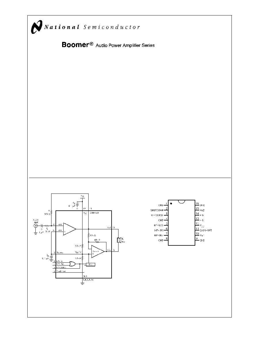
Typical Application
Connection Diagram
The Boomer
Æ
registered trademark is licensed to National Semiconductor for audio integrated circuits by Rockford Corporation.
Patents pending.
DS011988-1
FIGURE 1. Typical Audio Amplifier Application Circuit
Small Outline Package
DS011988-2
Top View
Order Number LM4860M
See NS Package Number M16A
August 2000
LM4860
1W
Audio
Power
Amplifier
with
Shutdown
Mode
© 2000 National Semiconductor Corporation
DS011988
www.national.com
Absolute Maximum Ratings
(Note 2)
If Military/Aerospace specified devices are required,
please contact the National Semiconductor Sales Office/
Distributors for availability and specifications.
Supply Voltage
6.0V
Storage Temperature
-65∞C to +150∞C
Input Voltage
-0.3V to V
DD
+ 0.3V
Power Dissipation
Internally limited
ESD Susceptibility (Note 4)
3000V
ESD Susceptibility (Note 5)
250V
Junction Temperature
150∞C
Soldering Information
Small Outline Package
Vapor Phase (60 sec.)
215∞C
Infrared (15 sec.)
220∞C
See AN-450
"Surface Mounting and their Effects on Product
Reliability" for other methods of soldering surface mount de-
vices.
Operating Ratings
Temperature Range
T
MIN
T
A
T
MAX
-20∞C
T
A
+85∞C
Supply Voltage
2.7V
V
DD
5.5V
Electrical Characteristics
(Notes 1, 2) The following specifications apply for V
DD
= 5V, R
L
= 8
unless otherwise specified. Limits apply for T
A
= 25∞C.
Symbol
Parameter
Conditions
LM4860
Units
(Limits)
Typical
Limit
(Note 6)
(Note 7)
V
DD
Supply Voltage
2.7
V (min)
5.5
V (max)
I
DD
Quiescent Power Supply Current
V
O
= 0V, I
O
= 0A (Note 8)
7.0
15.0
mA (max)
I
SD
Shutdown Current
V
pin2
= V
DD
(Note 9)
0.6
µA
V
OS
Output Offset Voltage
V
IN
= 0V
5.0
50.0
mV (max)
P
O
Output Power
THD+N = 1% (max); f = 1 kHz
1.15
1.0
W (min)
THD+N
Total Harmonic Distortion + Noise
P
O
= 1 Wrms; 20 Hz
f
20 kHz
0.72
%
PSRR
Power Supply Rejection Ratio
V
DD
= 4.9V to 5.1V
65
dB
V
od
Output Dropout Voltage
V
IN
= 0V to 5V, V
od
= (V
o1
- V
o2
)
0.6
1.0
V (max)
V
IH
HP-IN High Input Voltage
HP-SENSE = 0V to 4V
2.5
V
V
IL
HP-IN Low Input Voltage
HP-SENSE = 4V to 0V
2.5
V
V
OH
HP-SENSE High Output Voltage
I
O
= 500 µA
2.8
2.5
V (min)
V
OL
HP-SENSE Low Output Voltage
I
O
= -500 µA
0.2
0.8
V (max)
Note 1: All voltages are measured with respect to the ground pins, unless otherwise specified.
Note 2: Absolute Maximum Ratings indicate limits beyond which damage to the device may occur. Operating Ratings indicate conditions for which the device is func-
tional, but do not guarantee specific performance limits. Electrical Characteristics state DC and AC electrical specifications under particular test conditions which guar-
antee specific performance limits. This assumes that the device is within the Operating Ratings. Specifications are not guaranteed for parameters where no limit is
given, however, the typical value is a good indication of device performance.
Note 3: The maximum power dissipation must be derated at elevated temperatures and is dictated by T
JMAX
,
JA
, and the ambient temperature T
A
. The maximum
allowable power dissipation is P
DMAX
= (T
JMAX
- T
A
)/
JA
or the number given in the Absolute Maximum Ratings, whichever is lower. For the LM4860, T
JMAX
=
+150∞C, and the typical junction-to-ambient thermal resistance, when board mounted, is 100∞C/W.
Note 4: Human body model, 100 pF discharged through a 1.5 k
resistor.
Note 5: Machine Model, 200 pF≠240 pF discharged through all pins.
Note 6: Typicals are measured at 25∞C and represent the parametric norm.
Note 7: Limits are guaranteed to National's AOQL (Average Outgoing Quality Level).
Note 8: The quiescent power supply current depends on the offset voltage when a practical load is connected to the amplifier.
Note 9: Shutdown current has a wide distribution. For Power Management sensitive designs, contact your local National Semiconductor Sales Office.
LM4860
www.national.com
2
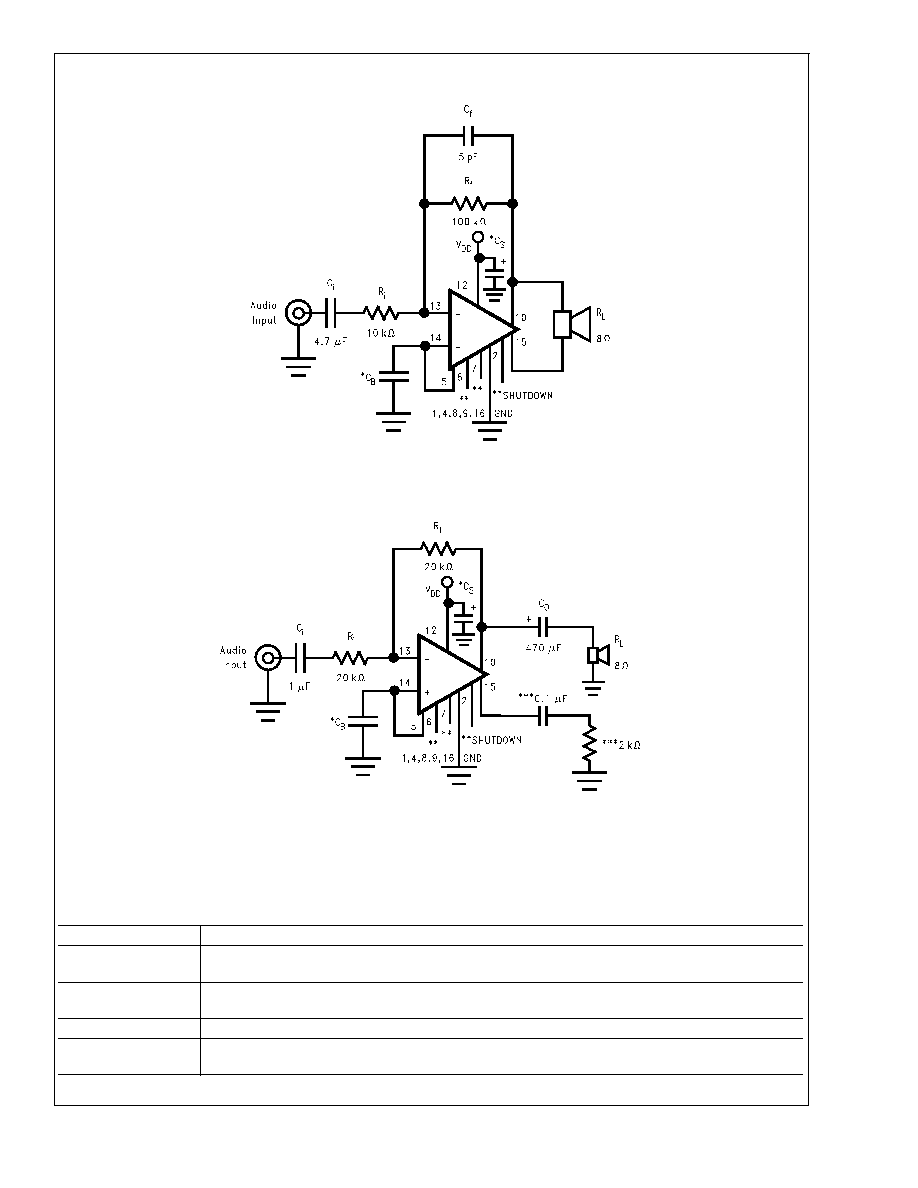
High Gain Application Circuit
Single Ended Application Circuit
External Components Description
(
Figures 1, 2)
Components
Functional Description
1.
R
i
Inverting input resistance which sets the closed-loop gain in conjunction with R
f
. This resistor also
forms a high pass filter with C
i
at f
C
= 1/(2
R
i
C
i
).
2.
C
i
Input coupling capacitor which blocks DC voltage at the amplifier's input terminals. Also creates a
highpass filter with R
i
at f
C
= 1/(2
R
i
C
i
).
3.
R
f
Feedback resistance which sets closed-loop gain in conjunction with R
i
.
4.
C
S
Supply bypass capacitor which provides power supply filtering. Refer to the Application Information
section for proper placement and selection of supply bypass capacitor.
DS011988-3
FIGURE 2. Stereo Amplifier with A
VD
= 20
DS011988-4
*
C
S
and C
B
size depend on specific application requirements and constraints. Typical values of C
S
and C
B
are 0.1 µF.
**
Pin 2, 6, or 7 should be connected to V
DD
to disable the amplifier or to GND to enable the amplifier. These pins should not be left floating.
***
These components create a "dummy" load for pin 8 for stability purposes.
FIGURE 3. Single-Ended Amplifier with A
V
= -1
LM4860
www.national.com
3
Single Ended Application Circuit
(Continued)
External Components Description
(Continued)
(
Figures 1, 2)
Components
Functional Description
5.
C
B
Bypass pin capacitor which provides half supply filtering. Refer to Application Information section for
proper placement and selection of bypass capacitor.
6. C
f
(Note 10)
Used when a differential gain of over 10 is desired. C
f
in conjunction with R
f
creates a low-pass filter
which bandwidth limits the amplifier and prevents high frequency oscillation bursts. f
C
= 1/(2
R
f
C
f
)
Note 10: Optional component dependent upon specific design requirements. Refer to the Application Information section for more in formation.
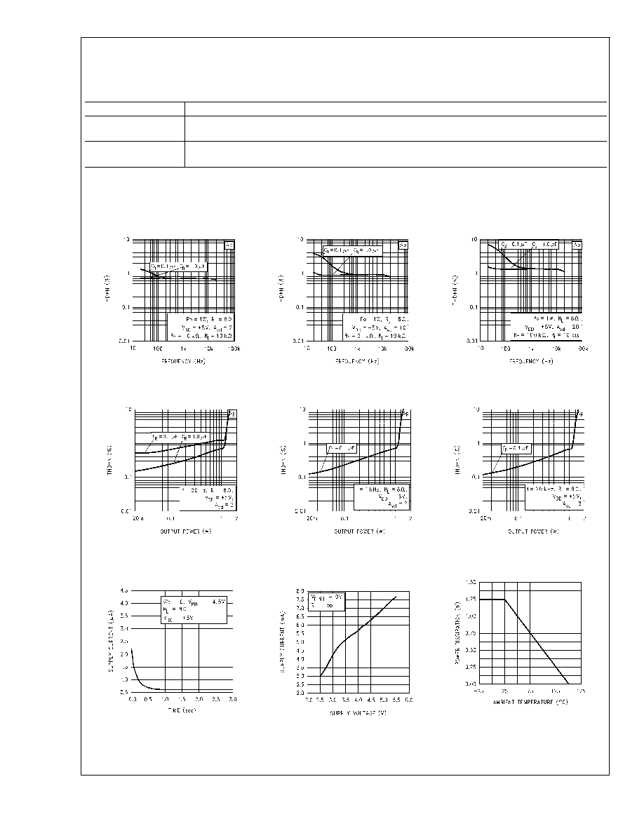
Typical Performance Characteristics
THD+N vs Frequency
DS011988-9
THD+N vs Frequency
DS011988-10
THD+N vs Frequency
DS011988-11
THD+N vs Output Power
DS011988-12
THD+N vs Output Power
DS011988-13
THD+N vs Output Power
DS011988-14
Supply Current vs Time
in Shutdown Mode
DS011988-15
Supply Current vs
Supply Voltage
DS011988-16
Power Derating Curve
DS011988-17
LM4860
www.national.com
4
Typical Performance Characteristics
(Continued)
Application Information
BRIDGE CONFIGURATION EXPLANATION
As shown in
Figure 1, the LM4860 has two operational am-
plifiers internally, allowing for a few different amplifier con-
figurations. The first amplifier's gain is externally config-
urable, while the second amplifier is internally fixed in a
unity-gain, inverting configuration. The closed-loop gain of
the first amplifier is set by selecting the ratio of R
f
to R
i
while
the second amplifier's gain is fixed by the two internal 40 k
resistors.
Figure 1 shows that the output of amplifier one
serves as the input to amplifier two which results in both am-
plifiers producing signals identical in magnitude, but out of
phase 180∞. Consequently, the differential gain for the IC is:
A
vd
= 2
*
(R
f
/R
i
)
By driving the load differentially through outputs V
O1
and
V
O2
, an amplifier configuration commonly referred to as
"bridged mode" is established. Bridged mode operation is
different from the classical single-ended amplifier configura-
tion where one side of its load is connected to ground.
A bridge amplifier design has a few distinct advantages over
the single-ended configuration, as it provides differential
drive to the load, thus doubling output swing for a specified
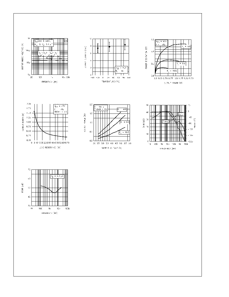
LM4860 Noise Floor
vs Frequency
DS011988-18
Supply Current Distribution
vs Temperature
DS011988-19
Power Dissipation
vs Output Power
DS011988-20
Output Power vs
Load Resistance
DS011988-21
Output Power vs
Supply Voltage
DS011988-22
Open Loop
Frequency Response
DS011988-23
Power Supply
Rejection Ratio
DS011988-24
LM4860
www.national.com
5